Whether you are a CPU collector, a vintage IC broker, a fan of old computers wanting to do some restoration work, or a hard-core geek trying to learn the fundamentals of classic microarchitectures, you should check the UCA! It can help you knowing more about antique technologies … or simply about the working condition of your ICs.
The Rise of Retrocomputing
A long time has passed since the 70s, when the microcomputing era began and integrated circuits started to spread all over the world. Some of them revolutionized our lives: the first 8088/8086 from Intel was introduced in 1978 before becoming the heart of the original IBM PC. Amazingly, the x86 ISA (Instruction Set Architecture) is still widely used today on modern Desktop CPUs! Even if these chips are long gone and not produced anymore for decades, there is still plenty of interest around them. Even better: the interest is growing, as the curiosity peoples for retro-computing is rising.
As a CPU collector, I'm always trying to find new CPUs I don't have. A chip certified working is much more valuable than in "unknown condition" or even worse, a defective one. Identifying failed or counterfeit ICs (they used to be common) can be challenging for various reasons. First, finding a test platform for a chip older than 20 years become more and more difficult. OId CPU/RAM/etc. are often still working well, but the well-known aging of capacitors, EEPROM or solder joints makes the failure rate of vintage motherboards very high. I'm not even mentioning the inevitable leaks of CMOS batteries or careless handling.
Introducing the UCA
I started to develop a tool to check my CPUs in summer 2017. The specifications were rather ambitious at first. I wanted an IC tester able to check as much different ICs as possible while keeping a small physical size. I also didn't want this project to use any obsolete support chip like clock generators, bus controllers or any hard to find components. Finally, I wanted a software upgradable tool (to add support for new chips or correct bugs without hassle). The idea to use a fast FPGA came as the only option because microcontrollers were too slow to interface at full speed with even a 8086 from the 80s. And I also wished to run the tested ICs at their rated frequencies. FPGAs have a lot of IO pins and can be software reconfigurable to accommodate a variety of pinouts. But modern FPGAs works with low-voltage TTL (3.3V) while old IC often want 5V and sometimes much higher voltage (i.e. up to 15V for a 4004). FPGAs are also expensive chips. To keep the whole system affordable, I use a main board (called "UCA") with pluggable "UCA Shields" (like in Arduino or Raspberry Pi) filled with low-cost voltage converters.
How It Works
Basically, the FPGA emulates the whole motherboard for the tested chip family. Clock generators, bus controllers, glue logic and many other original circuits (like reset or interrupts handling) has been recreated in HDL, then synthetized inside the FPGA. The RAM and ROM are also implemented the same way. Everything is integrated. A custom C or ASM code is written for the specific chip using an assembler, then initialized in the FPGA's ROM.
How It Is Built
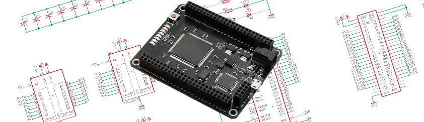
Developing a compact FPGA PCB with 100+ I/O is not extremely complex, but it's not cheap. You must use a 4-layer PCB (or more) and solder a fine-pitched QFP or BGA IC. In small quantities, the price skyrockets very quickly. So I looked at the FPGA development boards already available in the market. No need to reinvent the wheel if something suitable was already created and mass-produced. All the UCA's intelligence is inside the HDL code that emulates (almost) everything and doesn't require fancy electronics. I found the perfect board: The Mojo from Embedded Micro. It was a successful Kickstarter project launched in 2013 that raised more than $100k.
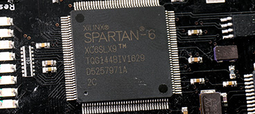
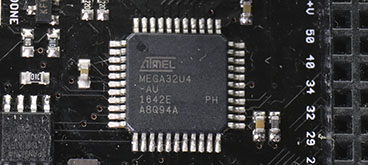
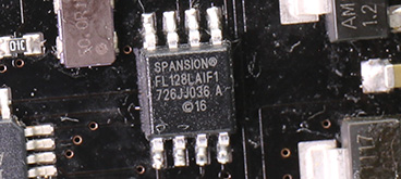
The Mojo is a simple board packed with an Atmel ATMEGA 32U4 microcontroller, 4 Mb Flash EEPROM and a Xilinx Spartan 6 FPGA. The XC6SLX9 model used is one of the most common FPGA. It has 9k logic cells, 576Kb of RAM blocks, lots of interesting features and 102 I/O. But the Mojo v3 wasn’t directly usable as the UCA because of its small EEPROM Memory (unable to store FPGA configurations for multiple shields) and too weak voltage regulation (to deliver a stable current for power hungry CPUs). To fit my needs, I modified the original Mojo to have 128 Mb of EEPROM Flash and a stronger voltage regulation. That only requires swapping some components but doesn't need any PCB modifications, so I was able to keep the original PCB layout. Of course, the original Mojo firmware burnt into the ATMega32U4 had to be rewritten, as well as the original FPGA firmware upload tool.
A Versatile Development Platform
Using the Mojo as the base platform, the UCA can be used as a generic FPGA development platform. Firmware Slot #0 is reserved for general purpose and automatically loaded when no UCA Shield is plugged. Two features from the original Mojo are not available due to pins being reassigned for other uses: A/D converter and USB serial output. If you need these features, it's still possible to flash a special "base" firmware very similar to the original Mojo Firmware. Some UCA Shields will not work anymore, but you can revert to the UCA firmware later. More interesting, the UCA can also be used as a development tool for the target vintage CPU. A compiled binary code can be uploaded and executed by the processor. A 8-bit output port linked to the UCA LEDs is available. Other I/O features will be available at a later time.