History
Everything began with that Shield. When I started this project, I had to choose the first CPU architecture to target. It was tempting to start with the MCS-4 (Intel 4004/4040) because those chips are the most valuable, but I don't collect non-x86 CPU myself, so I decided to start with the very first x86 CPU: The Intel 8086. It uses a multiplexed 20-bit address & 16-bit data bus. The 8086 is very close to the 8088 used in the original IBM PC, the latter being only a cost-down version with a data bus limited to 8-bit. I had to support both, as well as all pin-compatible CPUs like NEC V20/V30. The early revision of the Shield (v0.1 to v0.5) only supported Intel 8088/86. Starting with v0.6, all 40 pins connects to FPGA and virtually any CPU powered with +5V to pin 40 and GND to pin 20 can potentially be supported. The Intel 8085, based on a microarchitecture very different than the 8086, has been added with a simple firmware update some weeks later.
How It Works Internally
The 8086 requires many support components to work. The most important one being the Intel 8284 Clock Generator and Driver. It generates the odd clock frequency needed by the 8086 (33% duty cycle) as well as READY and RESET signals. I wrote an HDL replacement for the 8284 and I synthesized it inside the FPGA. Big advantage: it's possible to internally generate many different clock frequencies without any additional components. I choose 4 of them, selected by the 2 first dip switches of the CONFIG bloc (see below). I then wrote a complete bus controller in HDL to handle the multiplexed address/data bus. One of the tricky part was the detection of the correct data bus width very early after reset. I wanted the CPU to be fully addressed according to his capabilities (16-bit for the 8086). Then I needed some ROM to store the test code and RAM to read/write the stack and some test variables. Both as been created using 64K block memory from the Spartan-6 FPGA and interfaced to the 8086/8088 using the bus controller previously synthesized. I also added a pseudo output port (20h) linked to the 8 bits of the UCA LEDs. A classic x86 ASM code is finally compiled with NASM and the resulting binary is initialized inside the emulated ROM. Modifying the x86 binary is possible directly in the FPGA firmware.
How It Works Externally
The iAPX 86 UCAS is very simple to use. There are only a few dip switches needed to set different modes, but it's very important to respect the User's Guide. Even if any mistakes will trigger the embedded protections, please always check carefully the configuration before putting any IC in the Socket. Here are the basic hardware components used.
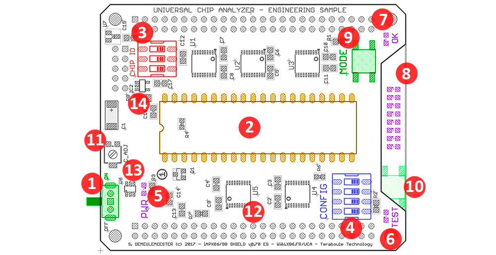
- Power Switch - Make sure the Shield is switched off before changing any dip switches, inserting or removing an IC! It's extremely important!
- IC Socket - A 40-pin ZIF Socket plugged into a soldered socket. ZIF Socket is replaceable if needed (damaged or worn-out). To reliably achieve clocks > 8 MHz, a high-quality ARIES Socket is used.
- CHIP ID Dip switches - The most important configuration on the iAPX 86 UCAS. Please make sure it's configured to the proper IC Familiy tester! (See below for more information)
- CONFIG Dip switches - Used to configure the Shield (set testing frequency, select burn-in or benchmark mode, ...). Check settings below for more informations.
- Power LED - Red LED. On when Power if applied to the IC, Off if unpowered. If power switch is ON and the Power LED doesn't lit, switch off the power immediatly: A short-circuit occured!
- Test LED - Orange LED. Blinks when CPU react to commands (linked to ALE signal)
- OK LED - Blue LED. On when a complete CPU test cycle has been done without errors.
- Status LEDs - 8-bit LEDs. Display a moving pattern when testing in progress, an error code if fixed, or diagnostics informations when the MODE button is pressed.
- MODE Button - When pressed, Status LEDs displays detection/diagnostic information (8088 Vs 8086 Vs V20 Vs V30). More to be added later (stepping detection?).
- RESET Button - Ask the CPU to initiate a clean reset and start a new test cycle.
- Current Adjust - A potentiometer used to set the highest current for over-current/short-circuit protection. Don't change it unless you're absolutely sure of what you're doing!
- IC - Level Translators - 5x Texas Instruments TXB0108. Bi-directionnal level converters to translate the +5V from the IC to the +3.3V needed by the FPGA, both way.
- IC - Protection IC - Texas Instrument TPS2552. Adjustable, Current-Limited Power-Distribution Switch. Supports up to 1.5A, but limited to a safe value with the potentiometer (11). Immediately power off the IC in case of short-circuit or unexpected high-current to avoid damages.
- IC - Current Shunt Monitor - Amplify the voltage drop in the shunt resistor. Required to monitor the power used by the device under test. Use the UCA in the tethered USB mode to get more infos.
Current & Futur CPU Family Supported
In addition of 8088/8086 and compatibles CPU, the iAPX 86 UCAS can also support other different CPU families. You will find below the current status. "Done" means the chip architecture is fully supported. "WIP" that we are working on it right now and "ToDo" that we will have to look at it later.
- Intel 8080 CPUs & compatible (Done)
- Intel 8085 CPUs & compatible (Done)
- Intel 8086 CPUs, NEC V20 & compatible (Done)
- Intel 8088 CPUs, NEC V30 & compatible (Done)
- Intel MCS-51 Microcontrollers (Done)
- Intel MCS-48 Microcontrollers (Done)
- Zilog Z80 (Done)
- RCA CDP1802/COSMAC (Done)
- Signetics 2650 (Done)
- MOS 65xx (WiP)
- Motorola 680x (ToDo)