When I designed the Universal Chip Analyzer, the goal was to be able to test everything from the 4004 to the 486 DX4-100 (and CPUs sharing the same pinout like AMD/Cyrix 5×86). Any Pentium-class CPU was out of scope due to physical limitation. Even if the UCA architecture can probably handle them from an electrical point of view, the size of adapters is just too small for the 200+ pins Socket needed for a Socket 4 or 5. Even the Socket 3 used by Pentium Overdrive on the PCB can’t fit between the two connectors. So P5 support on the UCA looked really impossible. Really? Wait a minute…
First, let’s have a look at the pinout of Pentium Overdrive, and especially at the outer pins rows :
 As we can see, all pins but 8 are reserved (No connection) or used for power supply (VCC/VSS). Pentium ODs requires much more power than any 486, so Intel basically doubled the number of power supply pins to insure stability. The INIT (F19) pin is basically useless because it’s redundant with RESET and supplied with an internal pull-down to avoid spurious trigger. The 7 others pins are related to Write-Back L2 cache, which is useless on the UCA because the internal RAM is as fast as the L1 cache. So maybe the Pentium OD can work without connecting the outer rows?
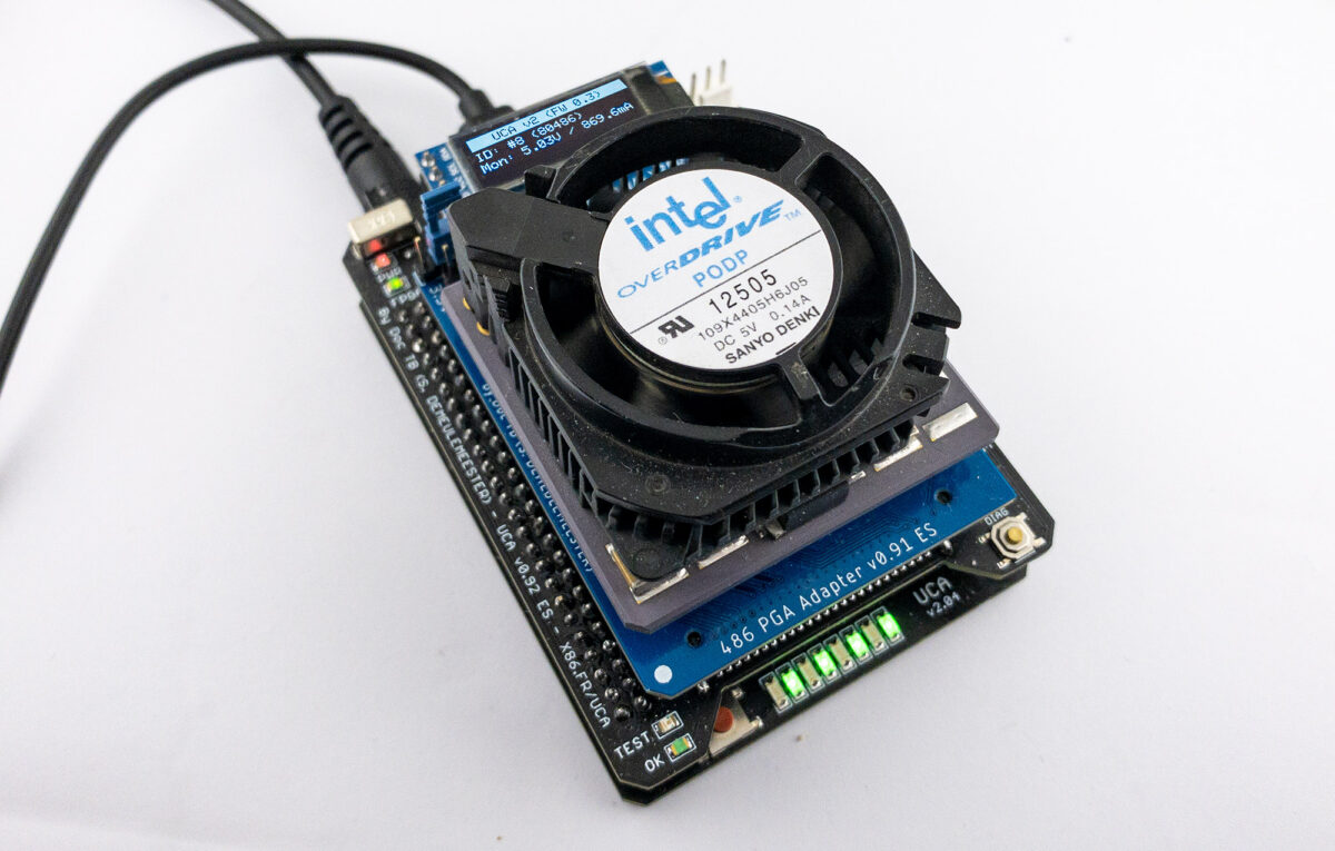
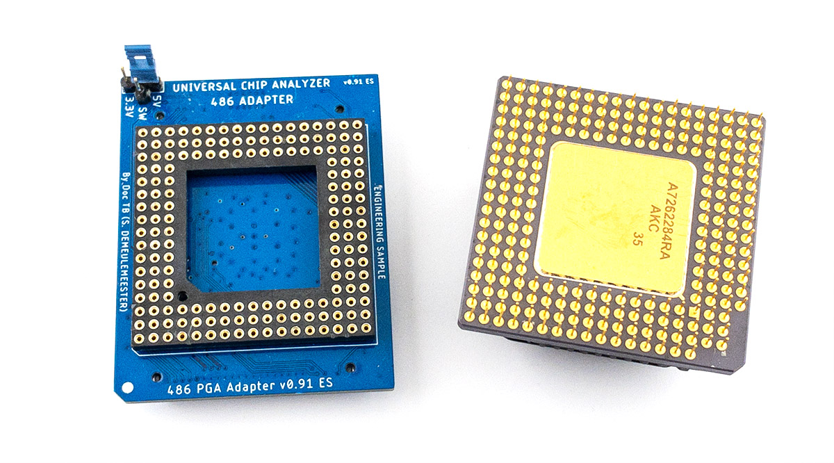
To check that incredible possibility, I build a 486 adapter with a standard Socket.
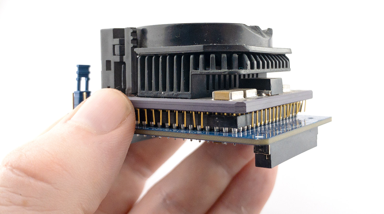
 The Pentium Overdrive 83 MHz fits perfectly with the outer pins floating.
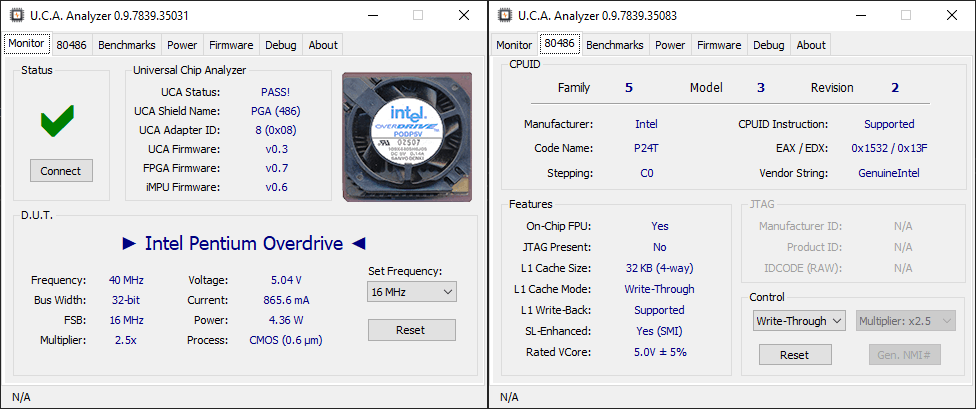
And … IT WORKS! At the UCA boot frequency (FSB 16 MHz), the CPU was able to run perfectly fine at 40 MHz using its internal 2.5x multiplier!
 After adding some code to support the new CPUID (0x1532), the UCA Analyzer tool was able to detect the Pentium Overdrive correctly and run the full test suite without issue.
 The Pentium OD doesn’t support JTAG, unfortunately. Power consumption is quite low for a Pentium-class CPU: 865 mA at 40 MHz. The last question is: how high can it go without the additional power supply pins connected? I tried 20 MHz FSB (50 MHz clock) without issue, then I tried 25 MHz FSB for a 62.5 MHz clock (like the Pentium Overdrive 63 MHz)
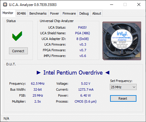 And it still works! Current consumption rises to ~1.3A to reach 6.4W. I also tried running the Pentium OD at full speed (33.3 MHz FSB for a 83 MHz final clock) but unfortunately, it only runs for a couple seconds before crashing. There is no doubt that the crash come from the missing power supply pins, but being able to run it at 63 MHz on the UCA is quite impressive!