![[UCA CPU Analysis] Prototype UMC Green CPU U5S-SUPER33](https://x86.fr/wp-content/uploads/2020/05/banner-2.jpg)
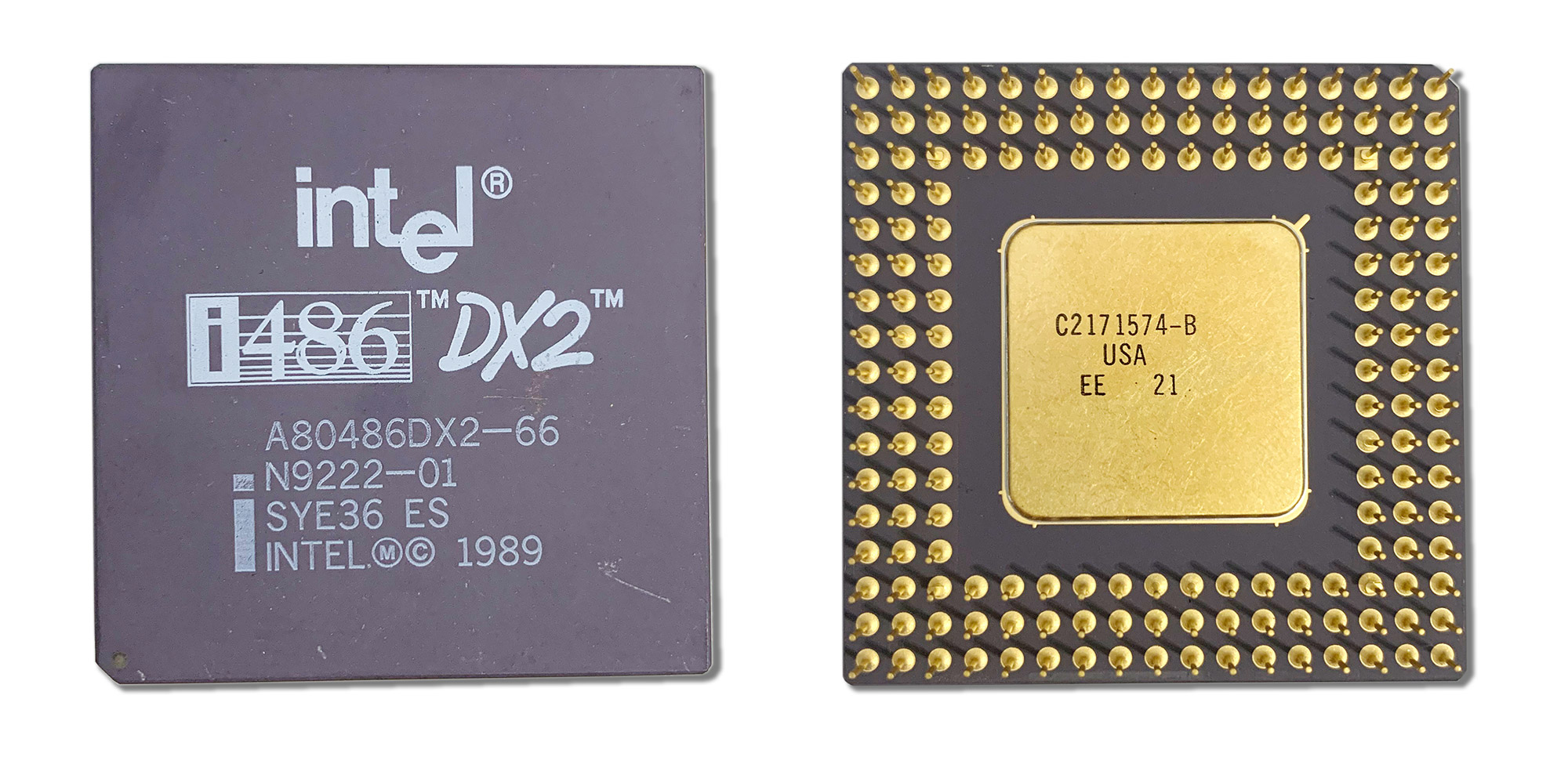
While sorting some new Engineering Samples I received lately, I exhumed some prototypes from my collection. They came without missing pins, so they are good candidates for an advanced investigation with the Universal Chip Analyzer.
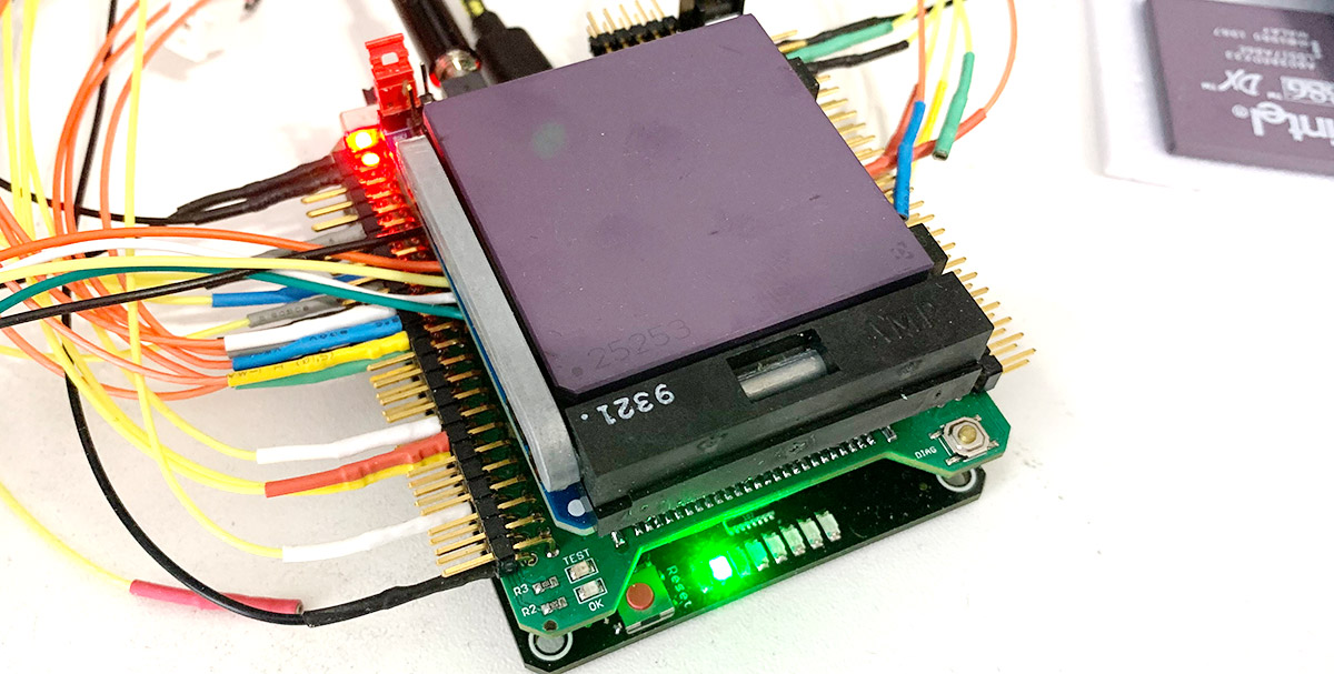
Let’s begin with the first one, a UMC Green CPU U5S-SUPER33
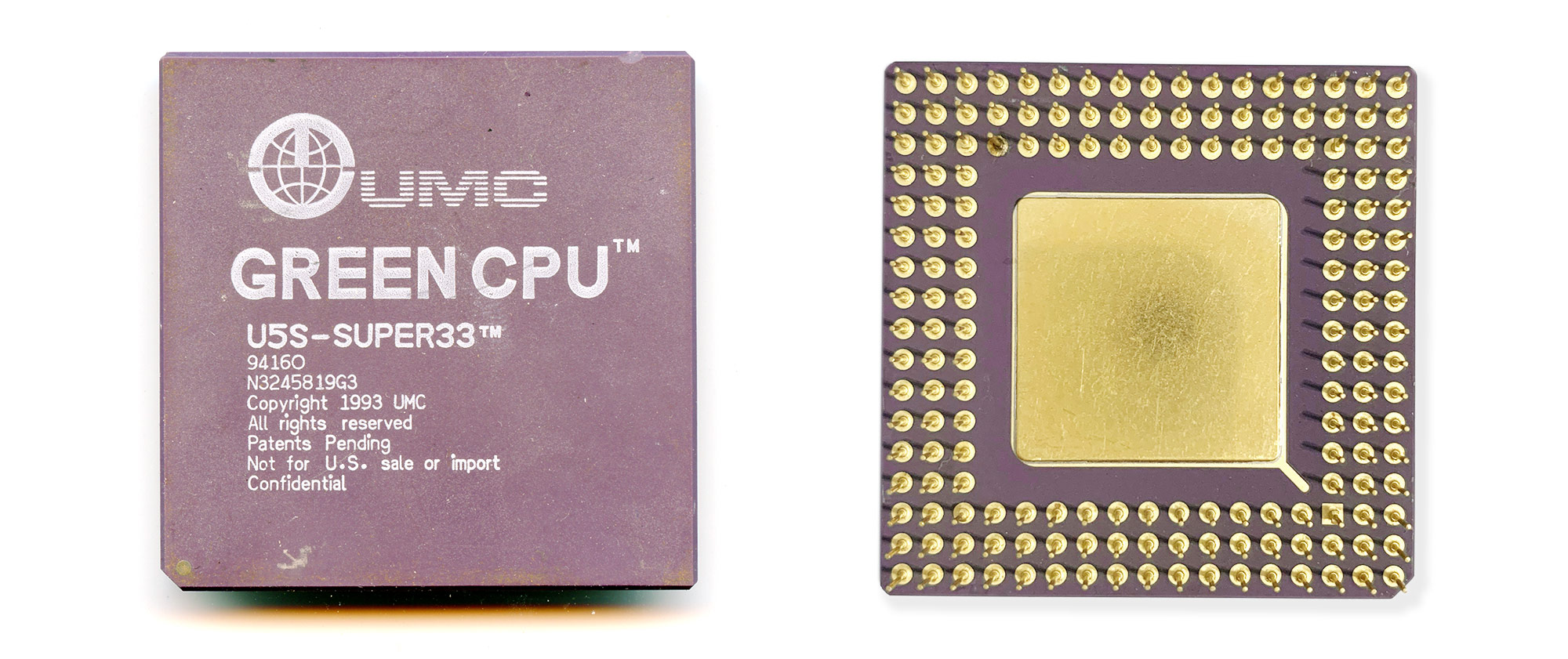 It’s marked “Confidential” on the last line, which means it’s an engineering sample. The date code is quite early: 9416. It was manufactured on the third week of April 1994. This CPU is not one of the very first samples of the whole U5S line regardless of the frequency, but probably a prototype for the specific 33 MHz version. Also notice the famous “Not for U.S. sale or import” line, written here because UMC was afraid – and rightly so – of the legal consequences of infringing Intel’s ‘338 patent.
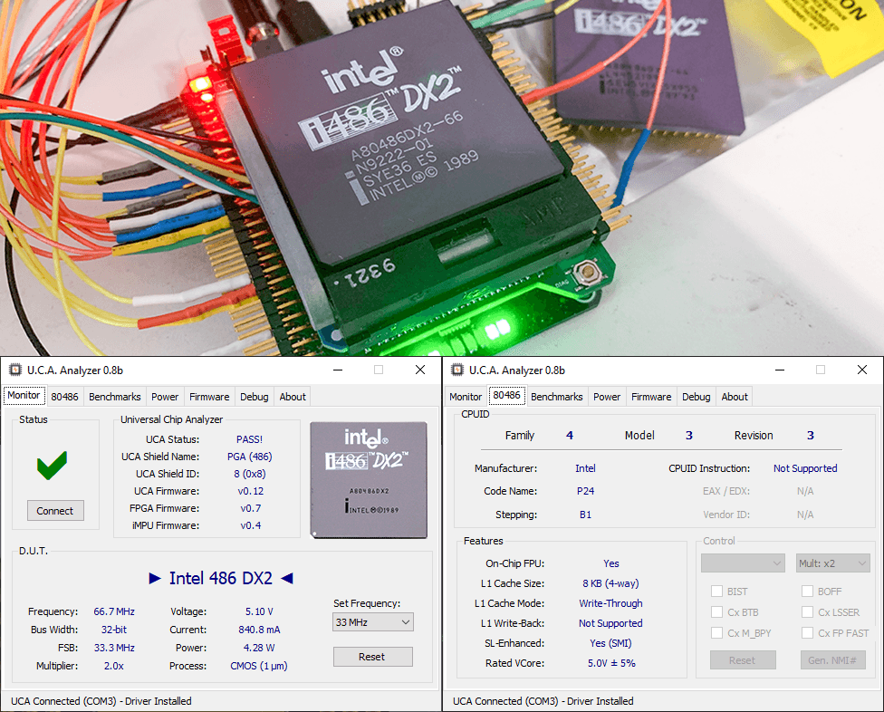
Let’s try it on the Universal Chip Analyzer:
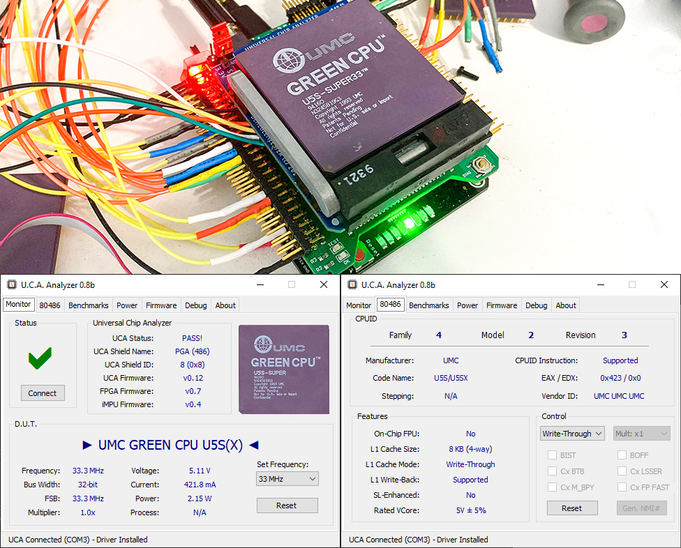 The prototype works fine up to 33 MHz. One of the first interesting points to check is the support of the CPUID instruction on such an early prototype. A few weeks ago, I was chatting with mtx500 (another well-known and very technical-aware CPU collector) about the way to detect UMC CPUs. He told me he uses the SALC/FS method to distinguish UMCs. The idea is to use the undocumented Intel opcode 0xD6 “SALC” (Set AL on Carry) instruction with the 0x64 “FS:” prefix. Only on a UMC, the combined 0xD6 0x64 opcodes return the “magic” constant 0x0AB6B1B07 in the EAX register.
I was wondering why to use this method when the CPUID instruction is supported? Mtx500 told me that early U5S might not support the CPUID instruction, so I was impatient to try on an early U5S like this one. It looks like the CPUID instruction is well supported, with the expected “UMC UMC UMC” string reported as well as the usual 0x423 family/model/revision on U5S(X). At first sight, this prototype looks strictly identical to the retail version. I ran some benchmarks to compare with later U5S and the cycle count of the test instruction flow is exactly the same.
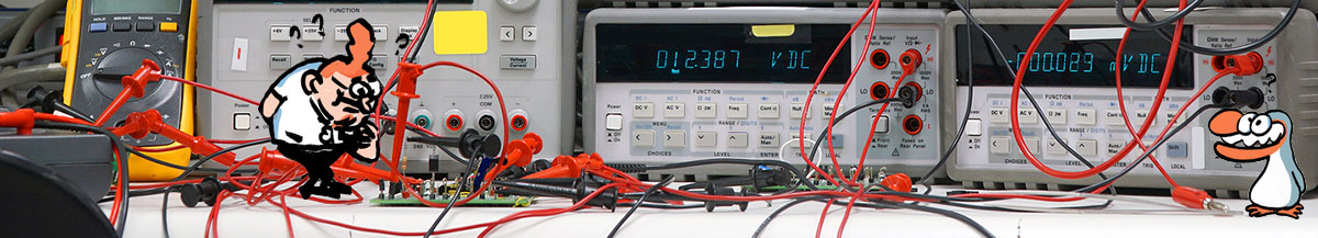
However, on closer inspection, I found a noteworthy difference: power consumption. I ran the same INT benchmark on my 4 U5S with the voltage set at 5.11V exactly on all of them. The UCA is quite precise at measuring power consumption. All of them were tested at a fixed 33.3 MHz frequency, no matter their rated maximum speed.
 The results are quite interesting. As you can see, all my retail U5S consume (almost) the same current: about 308 mA at 33 MHz while running my benchmark code. For an unknown reason, the U5SD is a bit higher at 321 mA, but the difference in power is only 50 mW. In the opposite, the prototype U5S-33 need MUCH more power to process the exact same code in the same time at the same frequency with the same voltage: 421 mA, which translate to about 2.15 watts.
The most obvious explanation is a switch in manufacturing process between the early prototype and the commercial revision. UMC was, at that time, one of the two major IC manufacturers in Taiwan, along with TSMC. We can consider they can switch easily between processes. On the very first U5S datasheet published in 1993, UMC indicates the U5S is built using a 0.6 µm CMOS process. This is consistent with the power consumption seen on the sample. I was able to find a table of the manufacturing process evolution in Taiwan in the 90s.
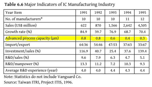 UMC and TSMC switched from 0.6 µm in 1993 to 0.4 µm in 1994. According to this table, it seems likely that the prototype is build using the ’93 process (0.6 µm) while UMC switched to the ’94 process (0.4 µm) for their retail mass-volume production. The retail U5S tested here need about 27% less power than the prototype. The theoretical reduction in power consumption between 0.6 µm and 0.4 µm is 33%, so that makes perfect sense. This Engineering sample is probably an early U5S manufactured with the original 1993 0.6 µm process. It is unknown at this point if retail (non-prototype) UMC Green CPU have ever been built with that process. Another analysis with a retail U5S produced earlier than August 1994 (Week 33’94) would allow us to be sure…
![[UCA CPU Analysis] Intel 486 DX2-66 SYE36 ES](https://x86.fr/wp-content/uploads/2020/05/banner.jpg)