The Intel 80186 is one of the lesser known early x86 CPUs. In February 1982, 4 years after the 8086’s introduction, Intel released its successor, the 80286 (or “286”). Simultaneously, Intel also quietly released the 80186 to target different markets. While the 286 is a generic microprocessor like the 8086 was, but based on a new microarchitecture, the 186 could be considered as the first x86-based microcontroller. The difference between a microprocessor (CPU) and a microcontroller (MCU) is the level of integration inside the chip. A microprocessor requires a lot of support components (memory controller, bus arbitration logic, etc.) and is primarily used to build computers. A microcontroller integrates many of these components along with a (less powerful) microprocessor and is used for embedded purposes.
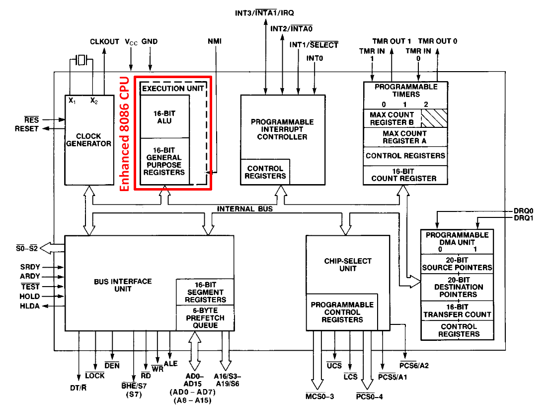
The 80186 integrates an enhanced 8086 CPU with a 16-bit bus and many support components: a clock generator, various controllers (DMA, Interrupt, bus, etc.), programmable timers, wait-state generator, chip-select logic, and even more. All these features greatly reduce the overall component count and the complexity of the board. Here is the original 186’s block diagram:
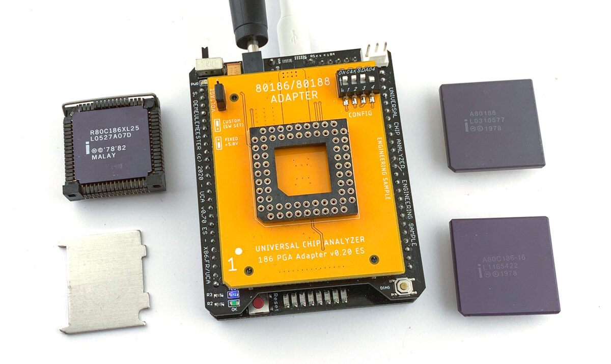
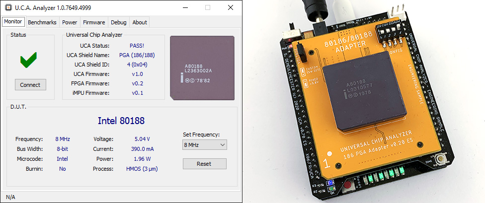
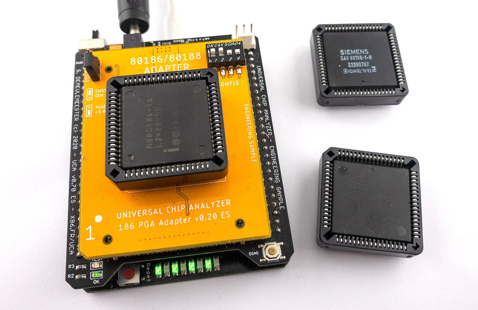
 The 80186 is basically a hybrid concept that has been used in embedded applications as a microcontroller, but also as a CPU to build cheap 8086-class computers. For example, it was at the heart of the Tandy 2000 PC released in 1983, but also buried inside the Intel 14.4EX Modem to compute complex algorithms. They later used the 80188, an even cheaper offshoot almost identical to the 80186 but based on an external 8-bit bus (like the 8088). As 8086-class CPUs, both the 80186 and the 80188 can be linked to the 8087 FPU, but this association was almost never found in real-world products. Original 80188/80186s were built on Intel’s HMOS 3 µm process at 6 MHz, 8 MHz and 10 MHz. They came in 3 different packages: PGA-68, leadless ceramic (CLCC-68) and leadless plastic (PLCC-68). The Universal Chip Analyzer is now able to test and run code on all these CPUs:
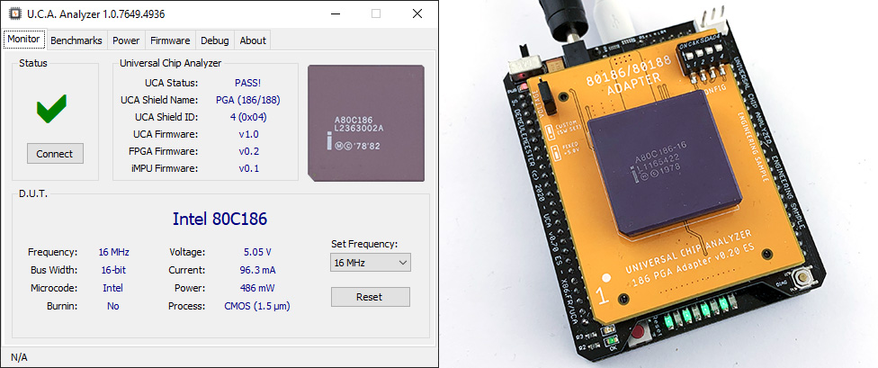
In 1987, Intel released the 80C188 and 80C186, built on Intel’s 1.5 µm CMOS process. Clock speeds reached 16 MHz and power consumption was vastly reduced. Some features were also added: a power-save mode, a refresh controller to handle RAM refresh cycle without external components and a FPU interface to support the newly released 80C187 (support for the old 8087 was dropped). The uncommon 80C187 is essentially a 80387 repackaged into a DIP-40 or PLCC-44 package. The UCA is able to test and detect 80C186 and 80C188 in various packages:
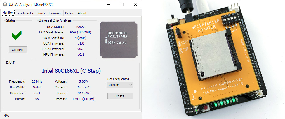
In 1991 (the 486 was available at that date), Intel released the improved “XL” variant. Thanks to the CMOS 1 µm process, the 80C186XL and 80C188XL were able to reach up to 25 MHz at a lower power consumption. They now use a static design (able to be clocked down to DC for even more power reduction) while the 80C18x were based on a dynamic design (with a minimum clock frequency needed to retain internal register values). The UCA can also test all members of the “XL” family and even detect their stepping (A-/B- or C-step) :
The maximum frequency for the UCA is 20 MHz because 186/188 requires a clock doubled input and I wanted to avoid an external PLL to keep cost low (the 186 adapter is a simple 2-layer PCB). Adding support for it to reach 25 MHz (or much more) is trivial but that will almost double the BOM price for the adapter (from ~$10 to ~$20).
Intel also released the 80C186EB (5V) and 80L186EV (3V) in 1990 and the 80C186/188EA & 80C186/188EC one year later (also available in ‘L’ version). The 80C186EA in PLCC-68 package is very close to the 80C186XL. The main differences are some more advanced power saving modes and TTL-level inputs compatibility (while the XL requires CMOS-level inputs). I’m still looking for one, but they should work fine on the UCA. The “EB” line adds an improved chip-select unit, two UART for serial communication and 16 GPIO. While electrically able to run on the UCA, they come in a bigger PLCC-84 and PGA-88 packages and don’t fit physically. The “EC” line adds even more GPIOs and is only available in SMD QFP-100 packaging. Designing an adapter for EB and EC 186/188s is not planned at this time.
Stay tuned for another big UCA milestone in the next few days!
PS: PLCCs 80188/186 are also supported!
RDC R8820 (and other of their 186/188 models), released ~2001, has “CPU ID” (https://html.alldatasheet.com/html-pdf/207355/RDC/R8820/110/2/R8820.html) – for me it’s not clear if that is CPUID or 386ID/EDXID/ResetID or something else?
100-pin QFP, so not for this shield, of course.