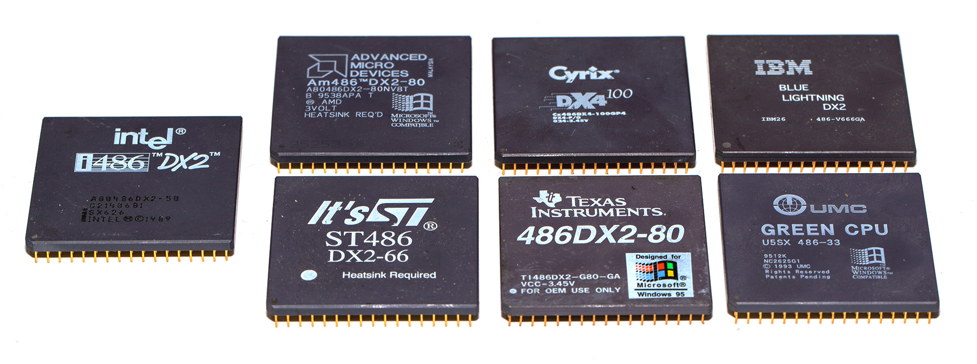
Released in September 1989 by Intel, the legendary 486 CPU enjoyed widespread popularity in numerous PCs for many years before being gradually replaced by the Pentium and its successors. This era profoundly influenced the entire CPU industry for decades. Up until then, only Intel designed x86 microarchitectures, allowing third parties like AMD to produce Intel’s intellectual property in their own fabs. However, in the first half of the 1990s, new CPU manufacturers emerged with their own 486-compatible CPUs, designed through clean-room reverse engineering. As a result, the decade was marked by numerous lawsuits between Intel and its new competitors over patent infringements related to the x86 architecture.
By the time Intel discontinued the 486 in 2007, the definitive list of pin-compatible 486 CPU manufacturers was as follows:
-
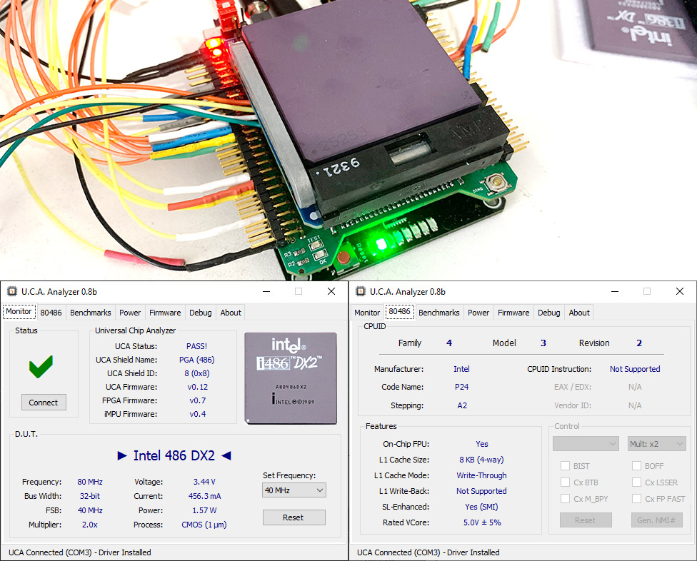
- Intel – The original developer of the 486, Intel released the 486, followed by the 486DX and 486SX (with a disabled FPU), then the clock-doubled DX2 and SX2, and finally the clock-tripled Intel DX4, reaching speeds of up to 100 MHz.
- AMD – Biggest second source. Produced both 486-clone based on Intel’s IP and in-house tuned architecture like the AMD X5 / 5×86 up to 160 MHz.
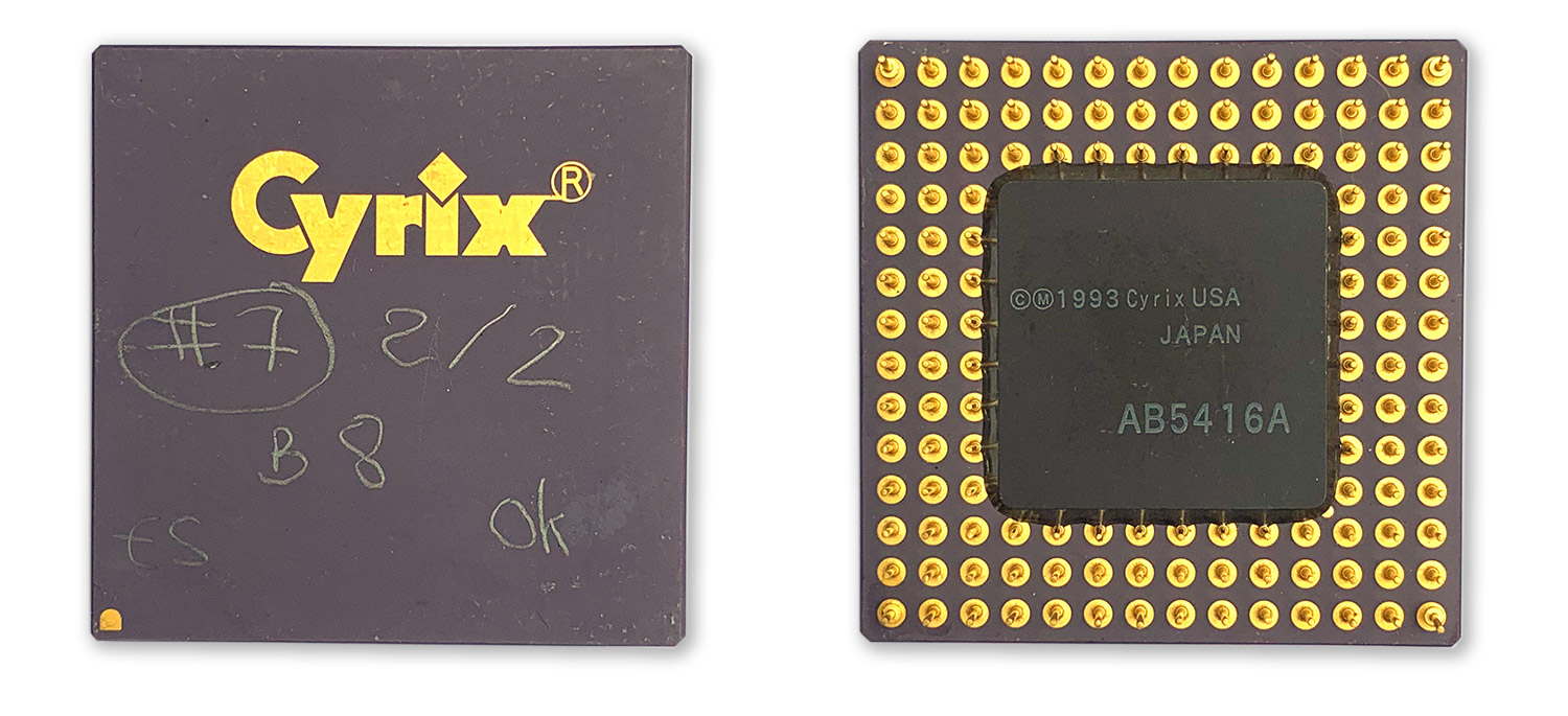
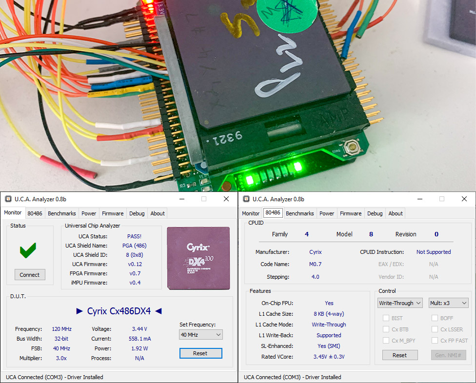
- Cyrix – Short-lived but famous company that only produced CPUs based solely on their own original designs, such as the Cx486 and the Cyrix 5×86.
- ST Microelectronics – Only rebranded Cyrix CPUs
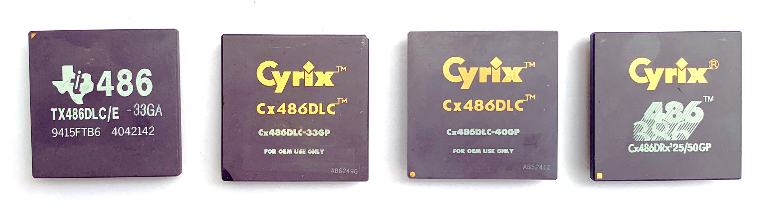
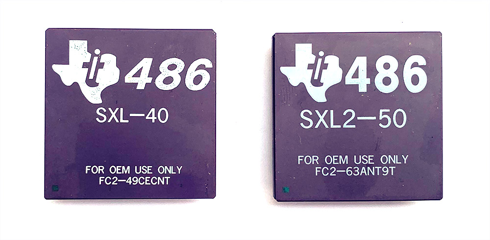
- Texas Instrument – Mostly rebranded Cyrix CPUs and a custom “barely compatible” 486 core (486SXL2)
- IBM – Mostly rebranded Cyrix CPUs, but also some Intel second source and even a custom 486 core internally used on IBM PCs (not on PGA)
- UMC – A Taiwanese company that produced some rare 486-compatible CPUs known as “Green CPU” using their in-house low-power microarchitecture.
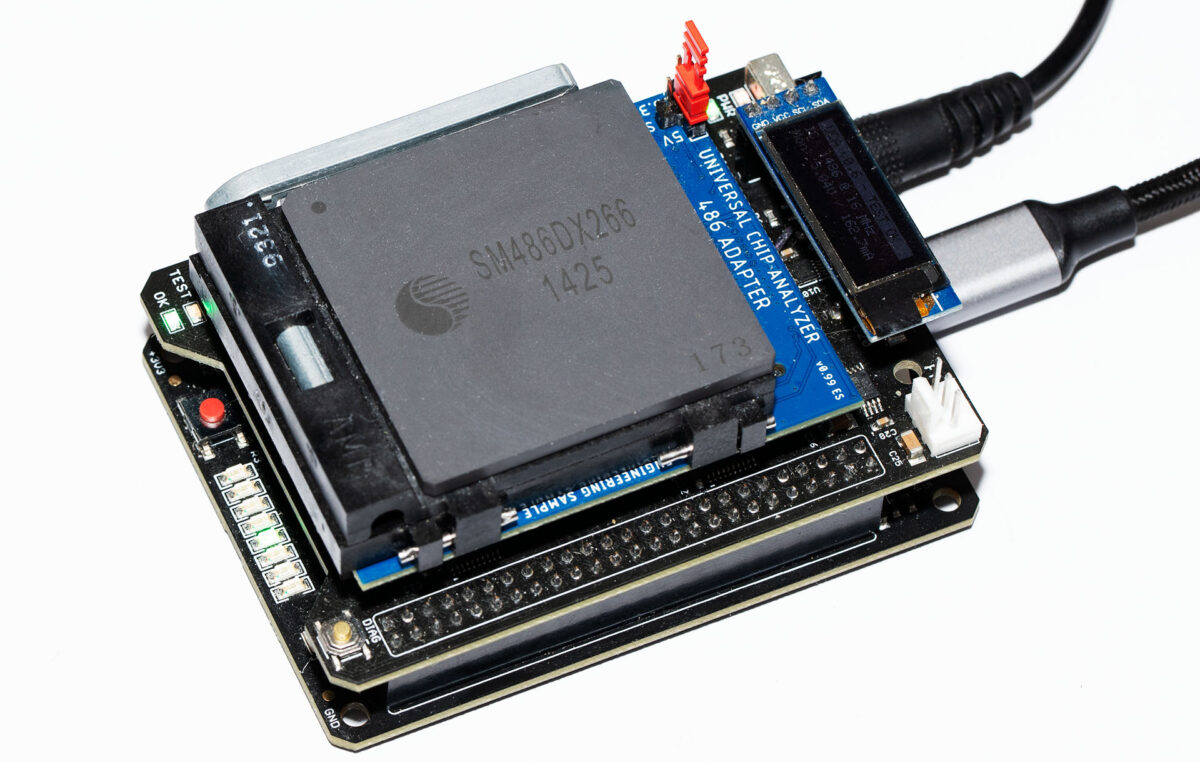
Although it is extremely rare to discover an unknown manufacturer of a well-known CPU like the 486, this is precisely what happened a few years ago when pictures of a peculiar and unseen 486 marked “SM486” surfaced online. Recently, I managed to acquire a couple of these elusive CPUs (a DX33 and a DX2-66). The Universal Chip Analyzer is the perfect tool for an in-depth study of these rarities. Are they merely clones of an already known 486 architecture? Are they based on a brand-new design? Where do they come from?
The story behind State Microelectronics
The first step is to identify the company behind the laser-printed logo on the CPUs. Given that they originated from China, a quick search on the Chinese internet revealed another picture of the logo with the acronym “SSMEC,” which stands for “Shenzhen State Microelectronics Co. Ltd.” This company was initially established in 1993 under the name “Shenzhen State Micro Science and Technology Co. Ltd.” It was the first IC design company to be part of China’s “909 Project,” a national initiative aimed at developing China’s semiconductor chip industry. The goal was to establish China as a competitive player in the global semiconductor industry, reduce reliance on foreign technologies, foster in-house innovation, and acquire Chinese-controlled intellectual property.
After numerous reorganizations over the years, SSMEC is now part of “Guoxin Microelectronics Co. Ltd.” a subsidiary of the state-owned giant Tsinghua Unigroup. Notably, Tsinghua Unigroup also owns “Yangtze Memory Technologies Corp” (better known as YMTC), the first Chinese-owned company to design and mass-produce the critical 3D NAND Flash used in smartphones and SSDs. I couldn’t find any reference to an x86 CPU developed by SSMEC on their (very undetailed) website. It’s difficult to determine exactly what this company is currently working on. The closest reference to a potential CPU is a 2011 award given by the Shenzhen Municipal Government for a “32-bit High-performance Integrated Communication Microprocessor.”
SM486DX33 Analysis
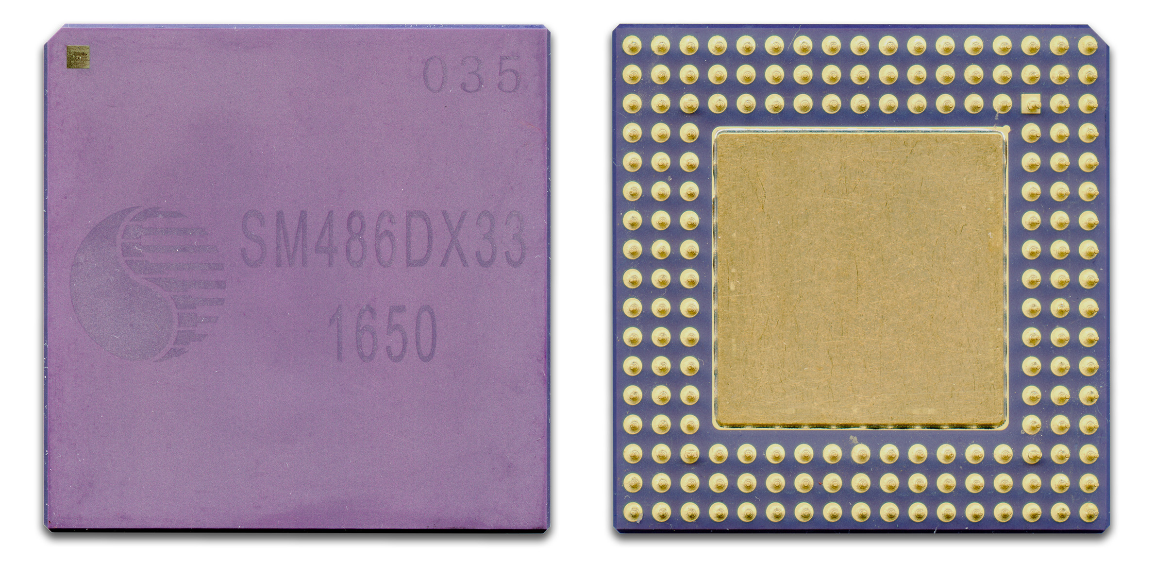
Physically, the SM486DX33 comes in a 168-pin PGA ceramic package. The printing is rotated 90° counterclockwise, but pin 1 is marked with a small square to ensure correct orientation. There are also two numbers laser-marked on top: “035” and “1650.” The latter appears to be a date code (Year 2016, Week 50), but 2016 seems quite late for a 486 CPU. Additionally, it appears that State Microelectronics changed its logo well before 2016. A 486-class CPU should have been produced in the 1990s, unless this chip was intended for a very specialized industry, such as aerospace or military. The back of the CPU has no markings, and the gold lid is slightly different from all other known Intel 486DX CPUs.
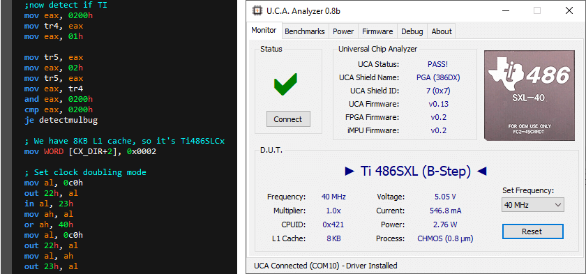
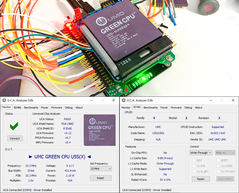
 For further investigation, let’s insert the SM486DX33 into the Universal Chip Analyzer. The first step was to determine the correct voltage. At 3.45V, the SM486DX33 only booted up to 20 MHz, so 5V was clearly the correct voltage to achieve 33 MHz operation. Both benchmarks ran successfully, and the UCA concluded the test with a PASS status. Here is how it is detected:
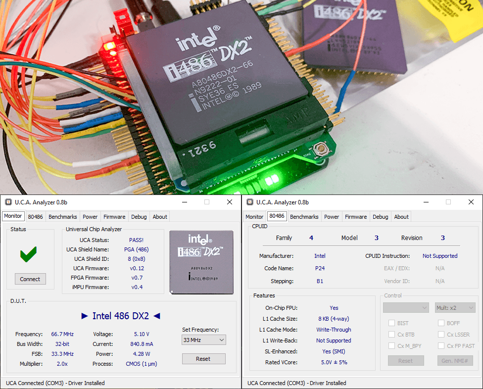
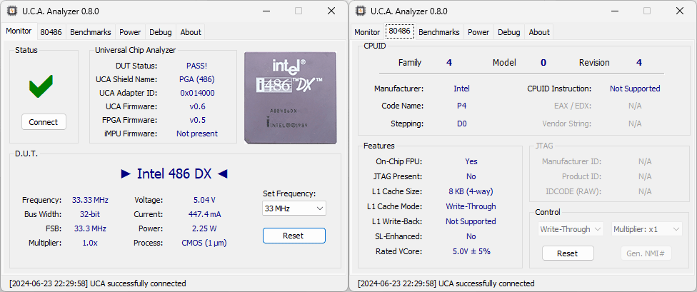
As shown in the screenshots from the UCA, the CPU is detected as an Intel 486DX with a reset signature of 0x404. The CPUID instruction is not supported, and JTAG is not available. The 0x404 identifier matches that of an Intel 486DX with the D0 stepping (either SX419 or SX729). It is very common for other manufacturers to copy Intel’s reset signature to avoid issues with software detection. However, a look at the benchmark results leaves no room for doubt: with an INT Benchmark score of 126.5 and an FP Benchmark score of 69.4, the SM486DX33 delivers exactly the same results as an Intel 486DX-33. All the INT/FP instructions have the exact same latency and throughput, indicating that the microarchitecture of this CPU is a perfect clone of Intel’s 486.
Now, we need to determine whether this SSMEC CPU is simply an Intel-produced 486 die assembled into a custom ceramic package, or if it is a clone built using a custom foundry process (possibly using Intel’s wafer masks). Again, the Universal Chip Analyzer can assist with its power-consumption profiling features. I compared the SM486DX33 with four different Intel 486DX-33 CPUs based on the D0 stepping, as well as with an earlier Intel 486DX-33 C0-Stepping and a later one built on the aB0 Stepping.
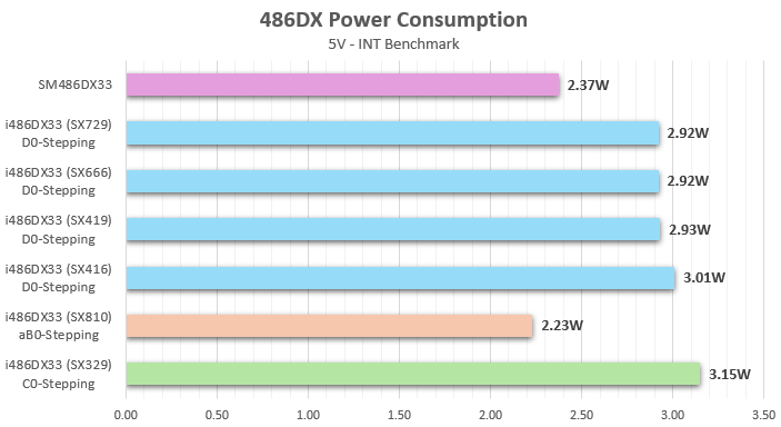
The results are quite interesting. All early Intel 486DX-33 CPUs up to the D0-Stepping are based on Intel’s P648 process (also known as CHMOS IV) with a 1 µm gate length. Later 486 models, such as the SL-enhanced SX810, use the newer P650 process (CHMOS V – 0.8 µm). At 33 MHz, the power consumption of an Intel 486DX built on a 1 µm node is 3.00 Watts +/- 5% (2.85-3.15W). Therefore, a 486 CPU returning the 0x404 (D0) signature should fall within that range. However, the SM486DX33 has a power consumption of 2.37W, which does not align with a 1 µm process, despite its signature. This suggests that the chip is built on a 0.8 µm process like the SX810, which has a 0x415 reset signature and supports CPUID and JTAG.
SM486DX266 Analysis
Now let’s examine the clock-doubled 486DX2 at 66 MHz from SSMEC. The top markings are similar to those on the SM486DX33, with two numbers: “173” and “1425.” As before, this appears to be a date code (Year 2014, Week 25) but could be misleading for the reasons previously mentioned. There are still no markings on the bottom, but the lid is much smaller, resembling the one found on later Intel 486DX4 models.
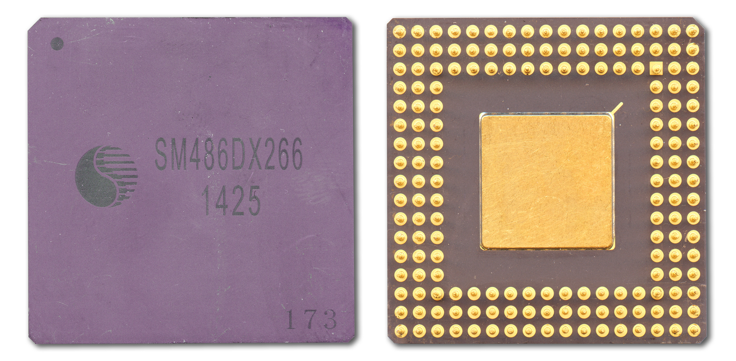 The SM486DX266 also operates only at 5V to achieve its rated speed. The UCA was able to test it perfectly. Here is how it is detected:
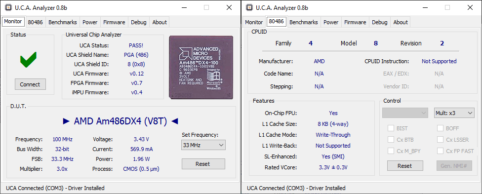
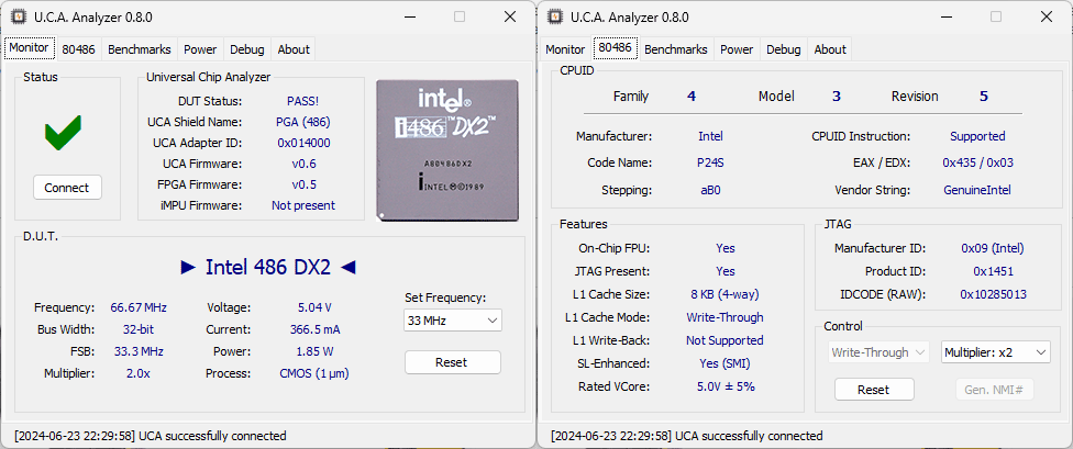 This time, the CPU from State Microelectronics is detected as an Intel 486DX2-66 (aB0-Stepping) with the 0x435 reset identifier, matching Intel’s specification. More interestingly, the CPUID instruction is now supported, confirming the 0x435 identifier. The CPUID Vendor String is “GenuineIntel,” just like on Intel’s 486 DX2. JTAG is also supported and returns Intel’s Manufacturer ID and the same Product ID code as the original DX2s. With an INT Score of 218.0 and an FP Score of 135.4, the SM486DX266 achieves the exact same results as an Intel 486DX2-66, indicating they share the same microarchitecture. Now it’s time to compare the power profile of the State Micro 486DX2 with Intel’s DX2.
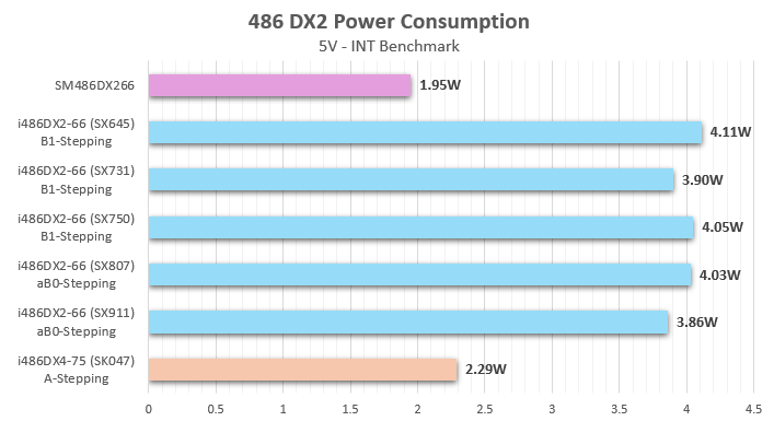
The results are surprising once again. The SM486DX266 requires half the power of any Intel 486DX2 based on the aB0-Stepping (SX807 and SX911). Intel’s aB0-Stepping (ID 0x435) is built on the P650 process (CHMOS V – 0.8 µm). However, the power consumption of the SSMEC CPU suggests it matches a more advanced process, such as the Intel P652 (0.6 µm) process used in later 486DX4 models. At 75 MHz, an Intel 486DX4 (0.6 µm) requires about 2.3W. When clocked down to 66 MHz, this almost perfectly matches the 1.95W of the SM486DX266. No genuine Intel DX2 CPUs have ever used a process more advanced than P648 (0.8 µm), making this finding quite interesting.
Conclusion
From a microarchitectural perspective, State Micro’s SM486s are clearly an exact replica of Intel’s 486 CPUs. The latency and throughput of instructions are identical between both CPUs. Even the JTAG identifier, which is the only way to distinguish between an Intel 486 and a third-party CPU like AMD using Intel’s masks, points to Intel. It remains unclear how State Micro obtained Intel’s 486 IPs and whether they had the legal rights to use them. Intel’s licensing of x86 products, especially during the 486 era, was extremely restricted. Only AMD and IBM had the legal right to produce 486s based on Intel’s IP, and that was granted after a long legal battle for AMD. It is highly unlikely that Intel would have granted such deep cloning rights to a state-owned company in China. Even if that were the case, they would likely have changed at least the JTAG identifier.
From a process standpoint, these SM486 CPUs reveal unexpected secrets. Both appear to be a node ahead of Intel’s genuine 486s (die-shrink), suggesting they likely did not come from an Intel fab. While the Intel 486DX-33 with D0-Stepping were built on a 1 µm process, the clone from State Micro seems to use a 0.8 µm (made-in-China) process. The same applies to the SM486DX2, which seems to be based on a 0.6 µm process, whereas Intel DX2s with aB0-Stepping were only based on the 0.8 µm process.
It’s possible that these CPUs were designed as test ICs to help establish a new Chinese foundry, which might explain their rarity and why they only surfaced in 2024. Another intriguing possibility is that they were produced to ensure long-term support for critical systems designed in the 90s, such as military applications, energy infrastructures (like nuclear or oil), or heavy civil technologies. For instance, many trains in France still use AMD 486DE2 processors as on-board computers.
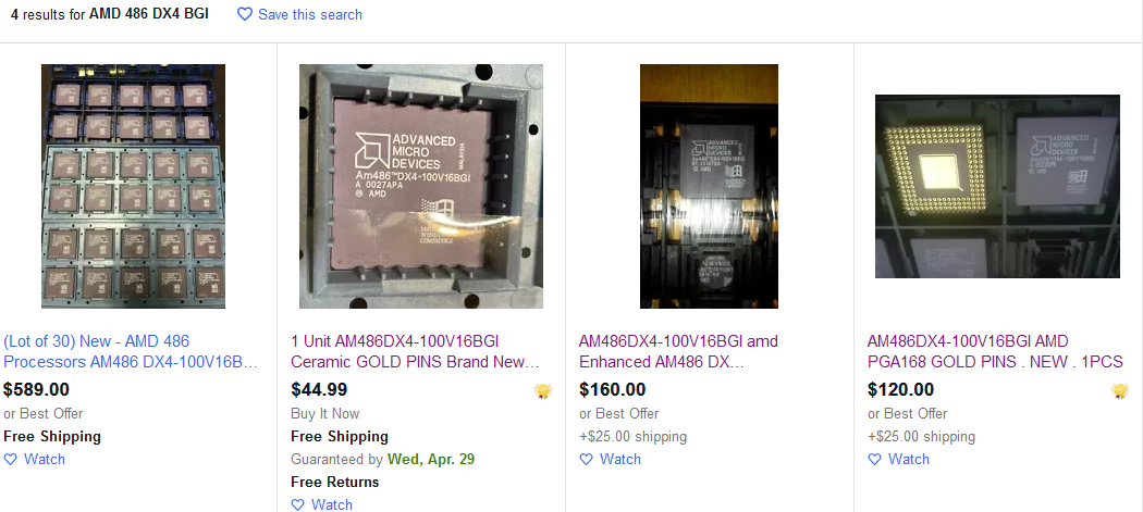
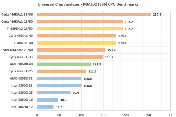
CPU collectors have observed a high demand for aftermarket microprocessors from the 80s and 90s from Chinese buyers since 2010. The most sought-after CPUs include the 80C186 and the 486DX33 and DX2-66 models. CPUShack, one of the largest resellers in the USA, who shipped over 1000 of these 486s to China, noted that the SX419 & SX729 (for DX33s) and SX807 & SX911 (for DX2-66s) were by far the most popular among Chinese buyers. These specific models correspond exactly to the D0 and aB0 steppings that the SM486 CPUs replicate. The exact applications of these 486s in China remain a mystery, but it’s clear that there is a significant and ongoing demand for them.
If you have any additional information about these chips, please contact me or leave a comment below – I’d love to hear from you!


![[Guide] Am486 Die & Packaging](https://x86.fr/wp-content/uploads/2020/07/allpackages-1200x622.jpg)
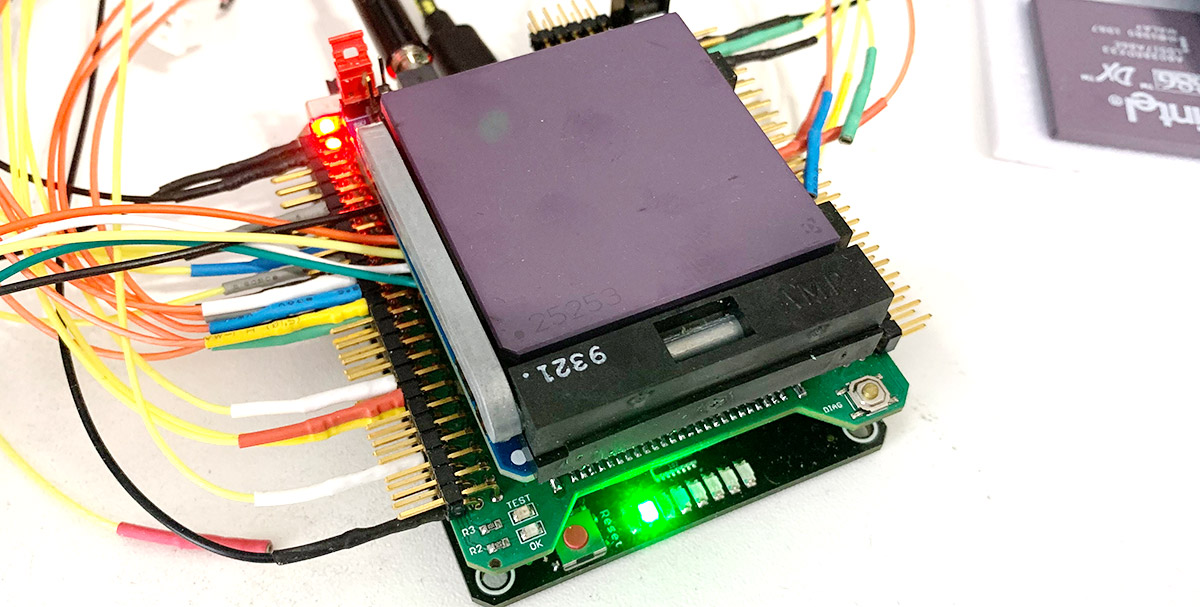
![[UCA CPU Analysis] Prototype UMC Green CPU U5S-SUPER33](https://x86.fr/wp-content/uploads/2020/05/banner-2.jpg)

![[UCA CPU Analysis] Intel 486 DX2-66 SYE36 ES](https://x86.fr/wp-content/uploads/2020/05/banner.jpg)
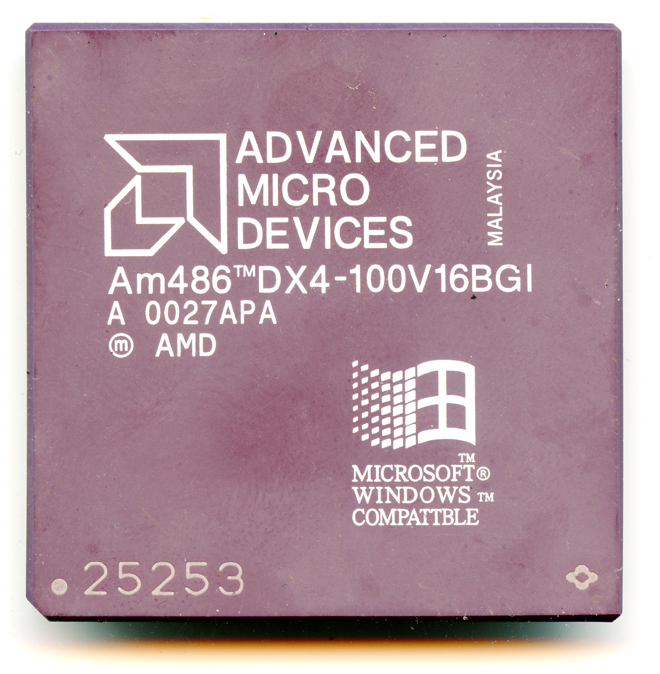
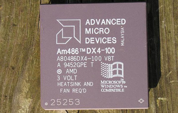
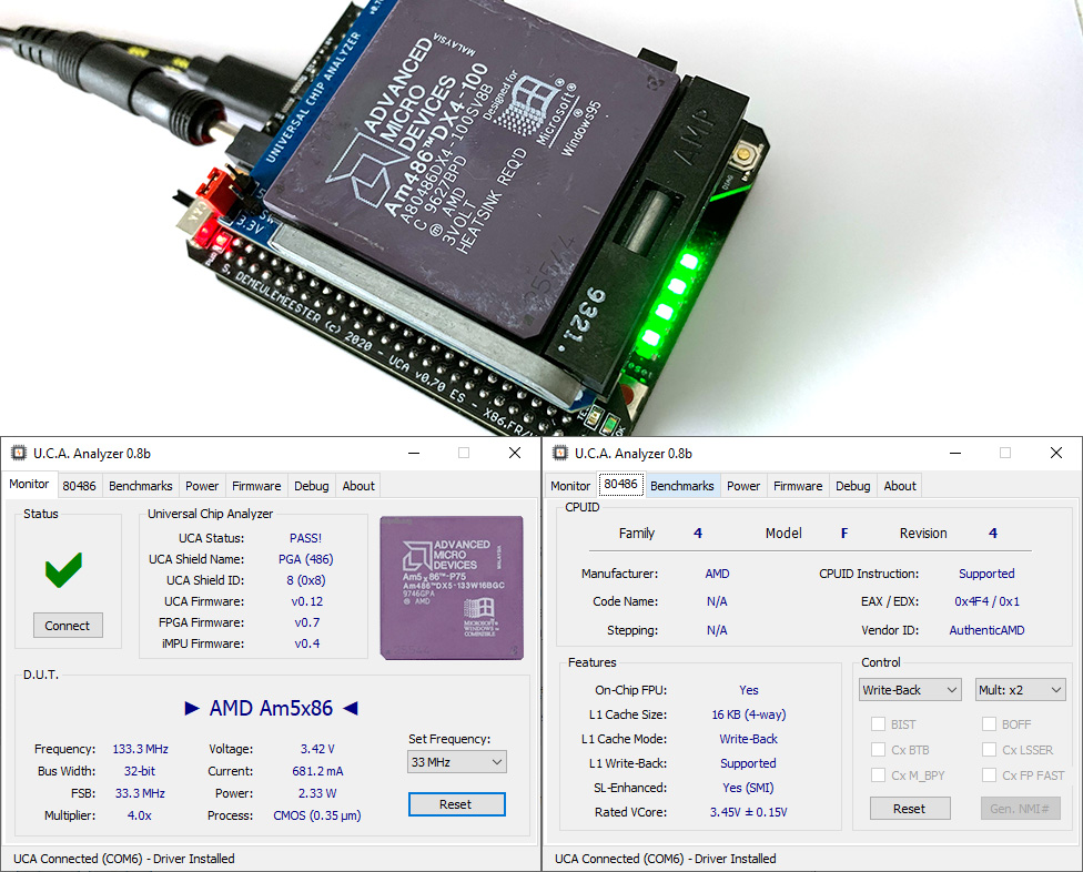
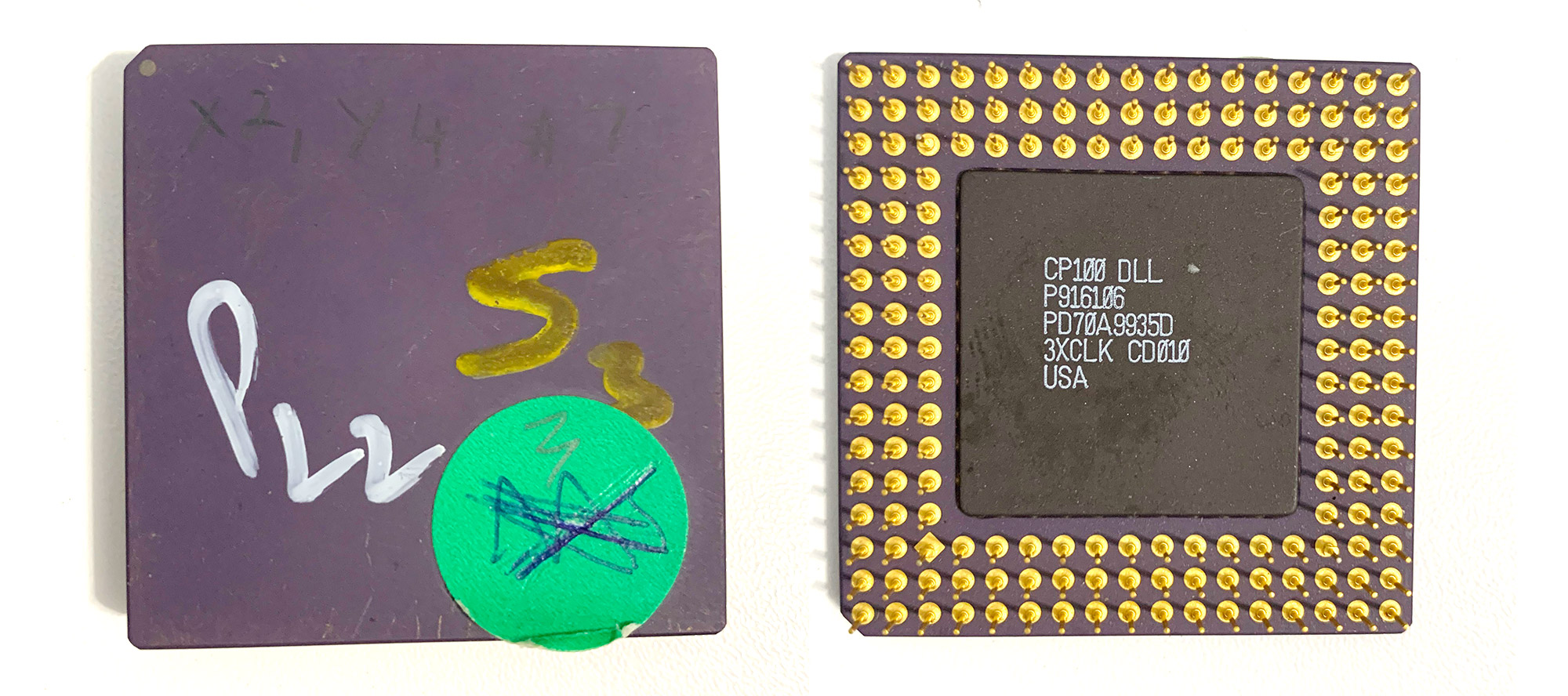
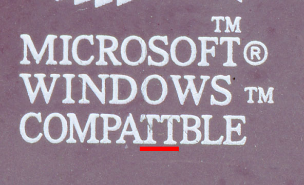 There is no doubt at this point that this CPU is a counterfeit Am486DX4. The only question remaining is when was it remarked by fakers? Counterfeits CPUs – especially 486s – were common in the 90s to boost frequency, but here, the original CPU was already an Am486DX4-100 (albeit a very early one with 8 KB L1 Write-Though Cache, instead of the expected 16 KB L1 Write-Back Cache). More recently, in the mid-2010s, old CPUs from the 90s were also faked to target CPU collectors all over the world.