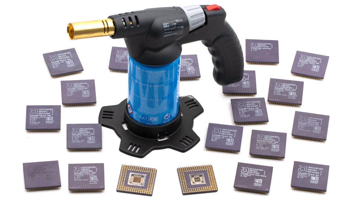
Working with the Universal Chip Analyzer has so far been a fantastic way to explore many aspects of the silicon industry from the 70s to the 90s, with a countless amount of details that remain to be learned. Lately, a reader told me about some strange 486s he had and was glad enough to lend them to me for a detailed investigation with the UCA. I can’t wait to tell you more about these, but I took some time first to write a complete guide to AMD 486 dies and packaging. I bought a LOT of Am486s and decap’d many of them to get some information. I also had the chance to talk with a former AMD engineer that worked on the Am486 product line back in the 90s.
Packaging (Style & Manufacturer)
A microprocessor is made up of a die (the small piece of silicon where the transistors are etched) assembled inside a package. Until the mid-90s, CPU manufacturers mainly used ceramic packages. This material is very hard, durable, and electrically non-conductive while able to dissipate heat fairly well.
The ceramic substrates used on Intel 486 processors were not made internally but bought from third parties, especially these four Japanese companies:
-
-
-
- Kyocera, who was known until 1982 under the name Kyoto Ceramic Company. By far the biggest company and the principal contractor. Others being mainly second-source alternatives.
- NTK Technical Ceramics, a subsidiary of NGK Spark Plug, a well-known manufacturer of isolators for the automotive industry located in Nagoya, Japan.
- Sumitomo Metal Ceramics, created in 1991 in Mine, Japan from parent company SMI (Sumitomo Metal Industries). Now owned by NGK.
- Shinko Electric Industries, the smallest of them, specialized on semiconductors packages in Nagano, Japan.
-
-
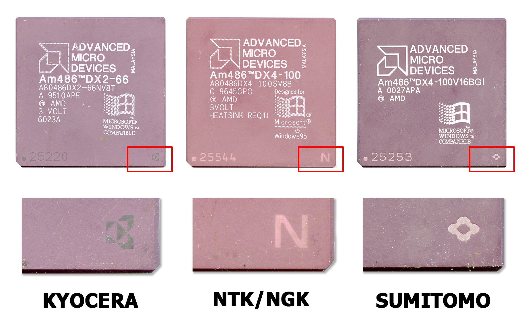
AMD ordered the substrates for their Am486 from the same companies, except for the last one. It’s very difficult to distinguish an Intel package manufactured by Kyocera from another one made by NTK or Sumitomo. Fortunately, that task is far easier with AMD’s 486 because of the logo printed – or laser engraved – on the bottom-right of the package.
 In the second half of the 90s, beginning with late Pentiums (P54CS), Intel gradually switched from ceramic to plastic packages for their processors. The previous “big three” companies (Kyocera, NTK and Sumitomo) from the ceramic era were progressively discarded while Shinko gained recognition, along with the US-based Johnson Matthey Electronics (a company established in 1817!). But the most technically advanced manufacturer of plastic substrates for semiconductors – named Ibiden Co., Ltd – remained in Japan (Ogaki). AMD only transitioned from ceramic to plastic long after Intel, with the Athlon XP launched in 2001. All previous CPUs (486, K5, K6-1/2/3, Athlon, Duron) were still based on good ol’ ceramic substrates!
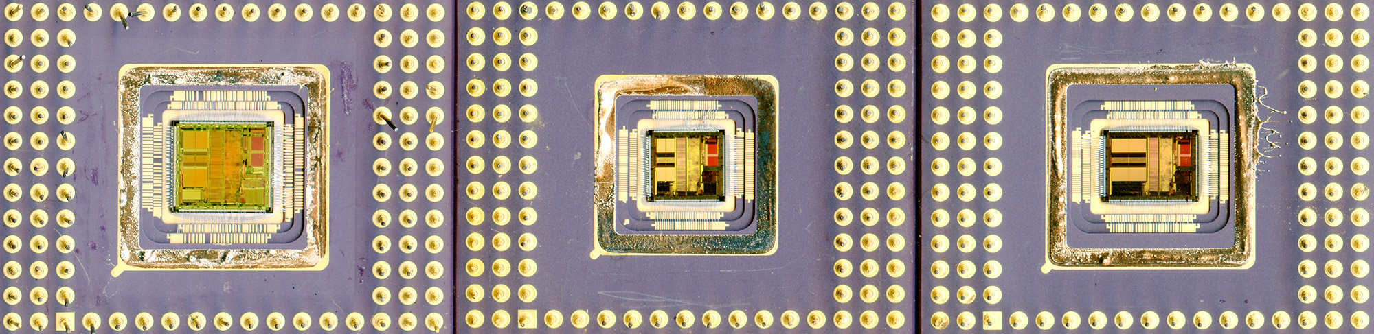
But let’s go back to our Am486. There are basically 2 major physical packages and 8 minor revisions. We’ll talk later about the minor versions, which can be recognized by their package code. The two major versions are distinguished mainly by the dimensions of the internal cavity, designed to accommodate the physical dimensions of a specific die. It’s easy to distinguish the two major versions by the size of the metallic plate that covers the die on the back of the CPU.
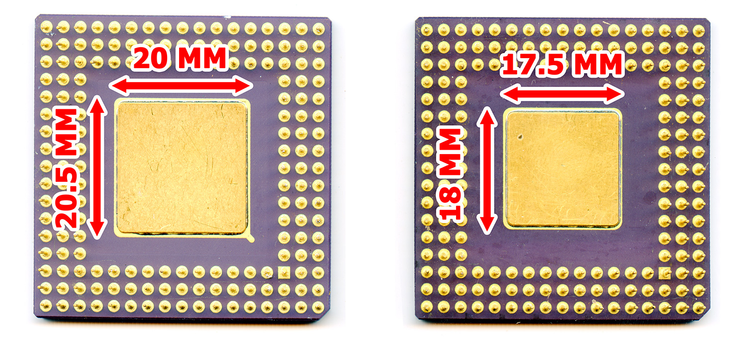
The size of the left one is 20 x 20 mm. The internal cavity can accommodate a larger die than the right one, which has a smaller cavity and a covering plate measuring only 18 x 18 mm. If you see the bigger plate on back, your Am486 is an early one with a bigger die. But if the plate is the smaller one, your CPU is probably a later one with a smaller die. Why are some dies small and others big? What’s the difference between them? Let’s dig deeper!
Dies & Process
Am486 dies were produced on 6-inch (150 mm) wafers. Depending on the manufacturing process, a single wafer can contain up to 200 dies. The more advanced the process, the smaller the transistors, and the more you can put on a single wafer at the same cost. Which means more profit.
 Today, AMD doesn’t have semiconductor plants anymore, their latest CPUs are manufactured by third parties (Samsung, TSMC, etc.) using processes far more advanced than what Intel is able to do. Since 2015, Intel has lost its technical advance for the first time in 40+ years and since then, Chipzilla has been unable to do better than 14 nm in big quantities, while the latest AMD Ryzen are based on a 7 nm process. Two steps ahead!
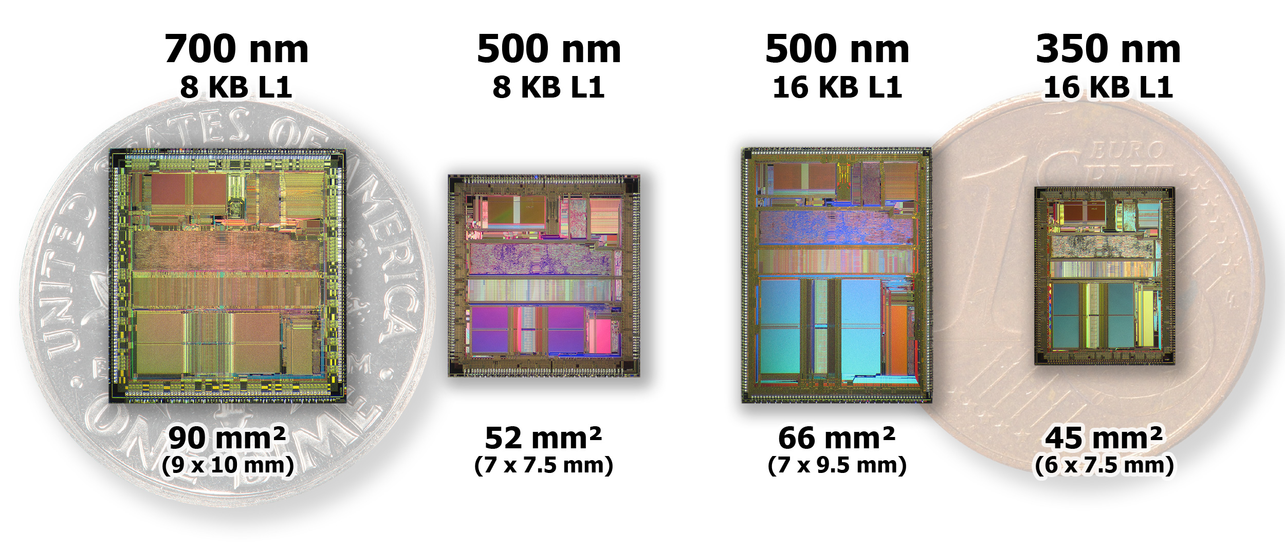
Back in the 90s, Intel was the unrivaled leader in manufacturing processes. When AMD announced the first Am486 DX on March 1993, it was made on a 700 nm process (each transistor was 100x bigger than the ones on the latest Ryzen!). At the same time, Intel had already produced CPUs with a similar process for 4 years and was readying 500 nm CPUs. During all of the 90s and 00s, the Behemoth from Santa Clara was always at least one process ahead of all its competitors.
Back to the Am486, AMD has manufactured four different major dies over the life of the product, each of them with numerous minor variations (steppings). For a better understanding, I put them (approximately) to scale:
-
- 700nm / 8KB – Manufactured since March 1993, the earliest one is the initial 700 nm die with 8KB of Write-Through L1 Cache for a physical size of ~90 mm². It was manufactured until mid-1995. Four retail steppings are known: B (Week 18 / May 93), C (Week 24 / June 93), D (Week 42 / October 93) and E (Week 12 / March 94). Stepping code “1D” and “E6” are not “real” stepping (ie: different masks from D and E) as they’re only based on small modifications on the bond-out pattern or a different way of binning. The specific E6 stepping is the same as E step, except the ICE (In-Circuit Emulation) feature has been fused down in response to an Intel trial agreement. All later steppings came without ICE microcode. All CPU based on A stepping (and many B as this stepping only shipped for some weeks) are engineering samples. All steppings integrate a clock-doubler PLL, but this feature was only enabled on some models (DX2s) and only starting with stepping D.
- 500nm / 8KB – In November 1994, AMD released the first die-shrink of the initial die at 500 nm, causing the size shrink down to ~52 mm². If you wonder why the die is so small, the answer is a better density (less space between transistors) along with the reduction of the transistors themselves. This specific die integrates a clock-tripler PLL (for DX4s) and the same 8 KB of L1 Cache from the previous iteration, but now with a Write-Back Mode. This feature requires some tuning on the package (additional pins are needed) and support from chipset manufacturers. Along with erratas on early revisions, it explains why the first steppings have write-back disabled. Three retail steppings are known: A (Week 46 / November 1994), B (Week 7 / February 1995) and C (Week 31 / July 1995). A suffix is sometimes present (AY, BC, CV) but does not indicate a different stepping. I couldn’t get any information on the modification done except for BC: a tiny modification on a pin was made at the request of a big OEM (Compaq) to fix a compatibility issue with a motherboard.
- 500nm / 16KB – This die is by far the rarest one. It’s the same as the previous one, still etched at 500 nm, but with 16 KB of L1 cache. The die size is ~15 mm² bigger. Only one stepping (B) is known, produced for some weeks between week 35 and 40 (~June 95). The yield (ratio between working and non-working dies on a wafer) was poor and AMD discarded almost immediately the production of this specific die with the full 16 KB cache enabled. Some CPUs based on this specific die were later released with 8 KB disabled.
- 350nm / 16KB – The latest and most advanced 486 die from AMD, a shrink down to 350 nm. While being almost the same 486 core as before, it now integrates 16 KB of L1 Write-Back cache and a clock-quadrupler (4x) PLL. The PLL is also able to work in 2x and 3x mode, depending of the specific model. Some of the Am486 built with this die can use a 2x/3x ratio (usually Am486DX4s) while others can switch between 3x and 4x (usually X5s / Am5x86s). Half of the cache can also be disabled on some models. Three retail steppings are known: A (Week 48, November 95), B(1) (Week 12, March 1997) and C (Week 3, January 1996). The last one being a specific stepping not directly related to the two firsts. I will tell more about it soon.
Package Codes
As of the Am386 and up to the Athlon 64s, all AMD processors have a 5-digit number written on their package for identification. This package code is closely related to the manufacturing process used.
-
-
-
- 700 nm 8 KB die
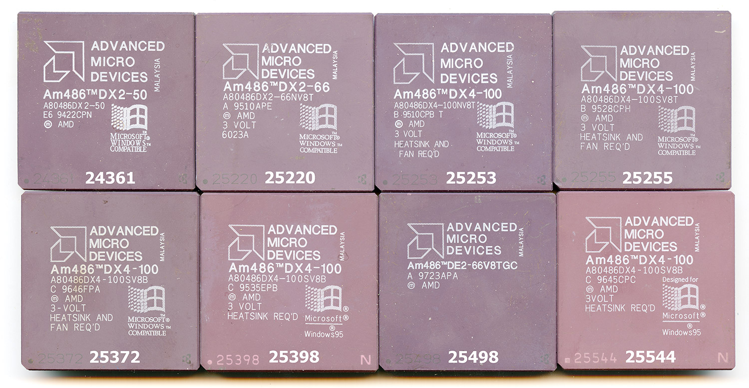
- 24361 – The very first package for Am486. Used from Week 15 / March 1993 (Engineering Samples) to Week 47 / November 1994. Stepping B, C, D & E were assembled with this package, for 5V CPUs ranging from the Am486DX-33 to late Am486DX2-80.
- 25220 – The second-generation package for the 700 nm die. Two different steppings were used inside this package: the last 5V die with stepping “E6” and the first 3.3V stepping “A”. The later has been produced until the end of 1995 for Am486DX2 at 50, 66 and 80 MHz
- 500 nm 8 KB die
- 25253 – The first package for the very common 500 nm / 8 KB die. Used from November 1994 to February 1996 for DX2-66 to DX4-100 (A Stepping) and DX2-66 to DX4-120 (B Stepping).
- 25255 – The second gen package, with the new pinout required to fully support SMI features but still based on a Write-Through Cache. AMD originally called these CPU “Am486Plus”. They’re quite rare and usually marked with the SV8T suffix. AMD produced them for 3 months (May-July 1995) before switching to the 25398 package that supports SMI and Write-Back cache.
- 25398 – The third gen package, only used with C Stepping from mid-95 to mid-96. Mostly DX4s were produced with this package, with only a few DX2s. The die is the first to have the die bonded-out to support Write-Back cache.
- 25498 – The last and newest package. It was only used for a short period (between May and October 1996) for the “old” C-Stepping and exclusively for DX4-100s. AMD also used this package for a much longer time (until 1999) for the specific embedded model Am486DE2-66V8TGC.
- 500 nm 16 KB die
- 25372 – This package is the only one available for the massive 500 nm die with 16 KB die. Two stepping are used: the very rare “B” stepping with 16 KB enabled was only produced for some weeks (marked “SV16B”), and the more common “C” stepping, with half of the cache disabled.
- 350 nm 16 KB die
- 25544 – The only package used for all late 486s built with the latest 350 nm process. They range from Am486DE2-66 to Am5x86. First engineering samples known are from October 1995 and the last ones were manufactured in 2003.
- 700 nm 8 KB die
-
-
AMD also released the later dies into a 208-pin SQFP (plastic) package for mobile and embedded computers.
Power Consumption
In order to grab as much information as possible about Am486 processes, I had to build a special firmware for the Universal Chip Analyzer. The goal was to be able to check the power consumption of all revisions (about 20 different ones!) at the exact SAME frequency and SAME voltage. That’s the only way to measure changes between two dies. Unfortunately, some Am486 requires 5V while later ones need 3.3V. Even worst, the same multiplier is not available on all parts.
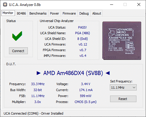
To solve the issue, I underclocked all the CPUs to 33.3 MHz at 3.45V. All 5V Am486s were luckily able to run reliably this way. To keep the frequency exactly the same, no matter the PLL multiplier set within the CPU, I configure the internal clock generator inside the FPGA for 33.3 MHz (1x), 16.66 MHz (2x), 11.11 MHz (3x) or 8.33 MHz (4x). So even a DX5-133 (4×33 MHz) ran at 4 x 8.33 = 33.3 MHz. Here are the raw results:
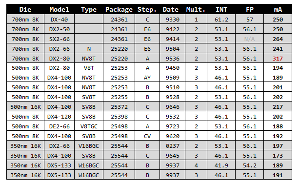
For each CPU tested, I checked the benchmark results to be sure everything was correct. I noticed that, while the FPU benchmarks remained almost the same no matter the multiplier, the INT benchmark slowed down a bit at each multiplier increase. This is probably due to the growing gap between the external front-side bus frequency and the internal ALU frequency, that led to an FSB bottleneck for simple (1- or 2-byte op) INT instructions. In real-world use, the clock-to-clock penalty was largely compensated by the much higher final frequency reached. Here is an easier to read chart:
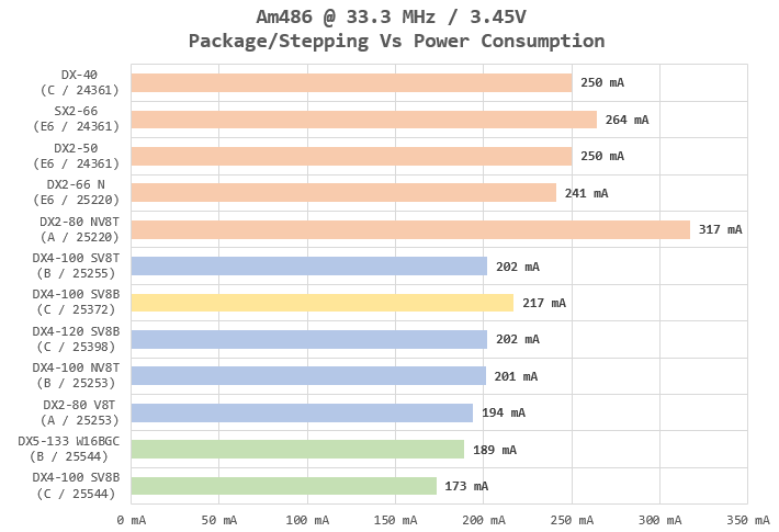
In orange, all the Am486s based on the first 700nm/8KB die. With the 25220/A excluded (will talk about this one later), the power consumption is consistent at ~250mA ±10mA. The standard die-shrink at 500nm (still 8 KB) reduces the power needed by -20% to ~200mA ±10mA (blue bars). The increased L1 on the elusive 500nm/16KB die (yellow bar) leads to a 10% increase. But keep in mind that my CPU had half the cache disabled. I’ll post an update here as soon as I’ll be able to put my hands on a fully enabled 25372. Finally, the last die (350nm/16KB – green bars) decrease the current requirement to ~180mA ±20mA, which is quite good considering the doubled L1 cache and the additional features.
The 25220/A mystery
When I started writing this, I had several questions about the dies present in different package. Power analysis answered a lot of them, and when doubts remained (ie: Is the 25372/C really based a stripped-down 500nm/16KB die?) I had to remove the protective cap covering the die to be 100% sure (ie: yes!). But one mystery remains…
Why the hell the 25220/A needs so much power? Removing the cap failed to provide an answer: the die seems to look the same than on older Am486 (25220/E6 and 24361). I bought 3x 25220/A from various sources and they all exhibit the same behavior. There is something strange with this stepping. The first 700nm/8KB started at B for Engineering Sample, then commercial CPUs had C-, D- and E- stepping. This “A-” stepping doesn’t make sense on that old 700nm die, as the earliest known 25220/A (Week 48’94) is actually newer than the earliest 25220/E (Week 44’94).
I can only make an educated guess at this time. Maybe AMD tested the RTL design planned for the 2nd gen 500nm die on the earlier 700nm process. That could have been useful to avoid shortages in case of later issues with the yield or production capacities on the 500 nm node. As soon as the 500 nm was up and running successfully (mid to late ’95), they were able to drop the old 700nm mask used on 25220/A. A die shot of the two die could help solve that mystery. I’ll post an update an soon as I know more…