When I started studying FPGAs more than two years ago to build a simple IC tester, I didn’t expect to support anything faster than the Intel 8086. The learning curve for Verilog has been quite harsh since then, but I’m now much more comfortable with complex logic, states machine and timings diagrams. I also learned a lot about how old CPU architectures work in depth and how to interface vintage circuit with modern hardware. Acquiring this knowledge step by step is quite exciting, even if I still have a lot to understand.
By the end of 2018, I was able to successfully interface an Intel 486 DX-33. That was quite a challenge and the HDL code was horrible (and the electronic as well, to be honest), but I knew that it was possible for the modest FPGA I use (a Xilinx Spartan 6 LX9) to support up to 32-bit architecture with quite fast bus frequencies and 0 wait state. Awesome!
* Now Truly Universal
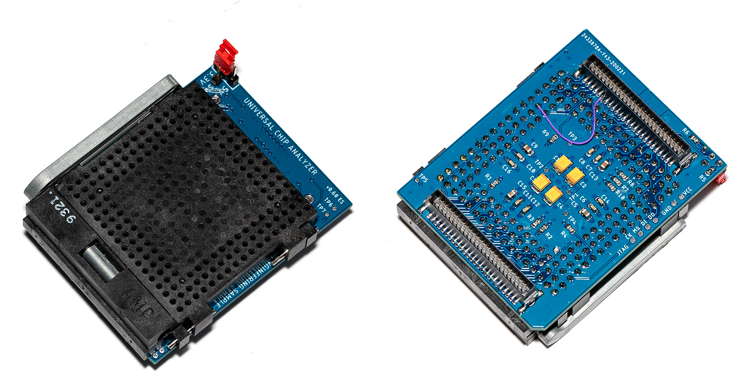
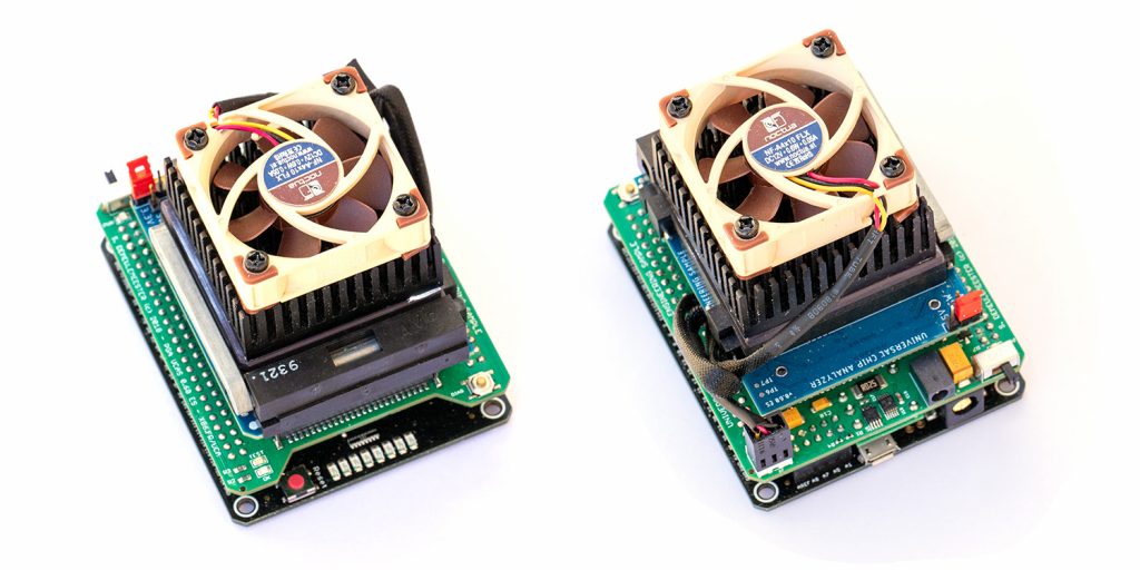
In 2019, I worked on a truly universal hardware platform that can support anything from the original Intel 4004 to much more advanced 32-bits CPUs like Motorola 68040 or Intel 486 (and also MCU, RAM, the Xeon ID platform and almost anything else). The goal was to raise (a bit) the cost of the UCA base board to keep the top adapters as cheap (and easy to design) as possible. The Universal Chip Analyzer now consists of a 3 layers stack.
-
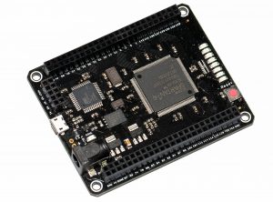
- The first (bottom) layer is still the modified Mojo V3 development board with the Spartan 6 LX9 FPGA. I thought for a long time about redesigning the board, but the embedded Micro team did quite a good job and cheap clones Mojo V3 are available. The main changes I made on the board are a much bigger Flash (256 Mb) to accommodate many different FPGA configuration files, a rewritten firmware to support all the new features and some tuning on the FPGA power stage.
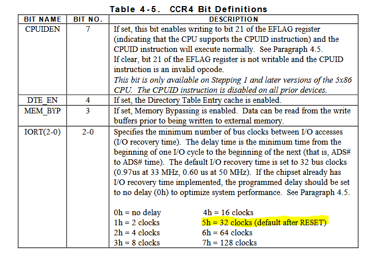
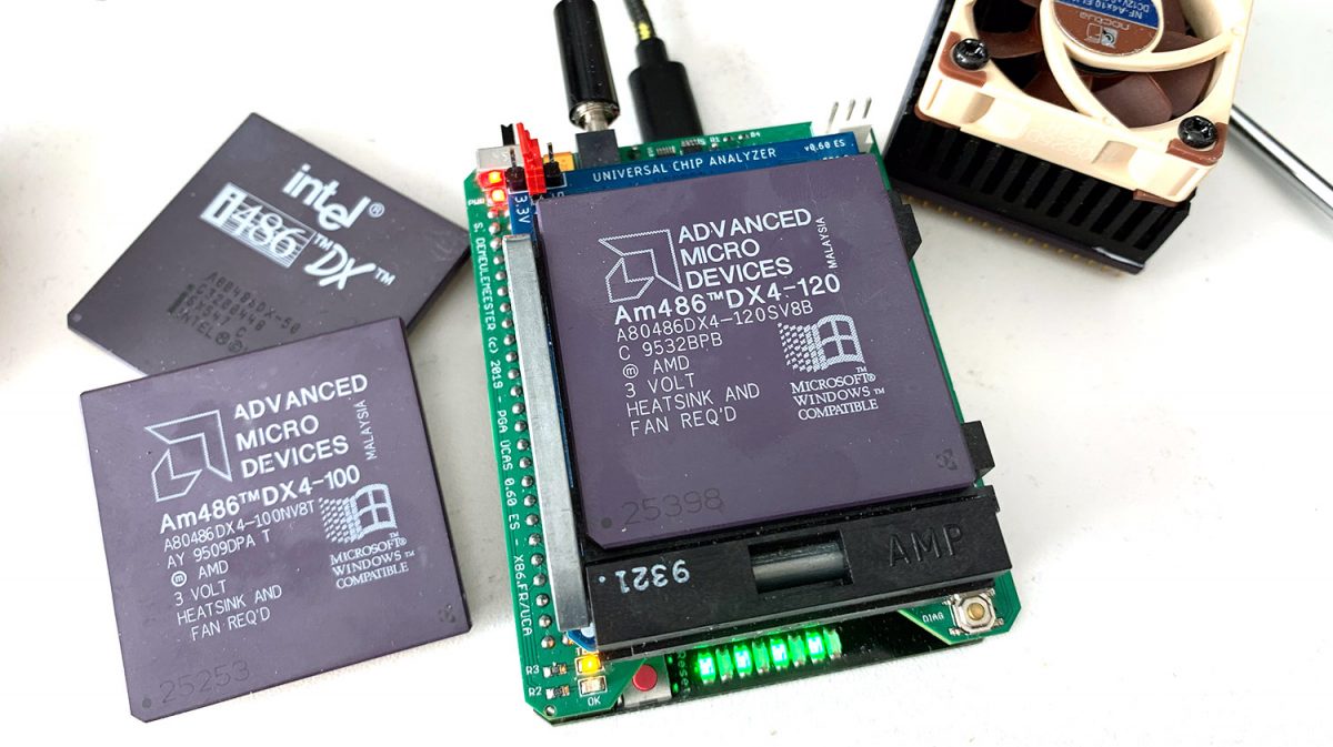
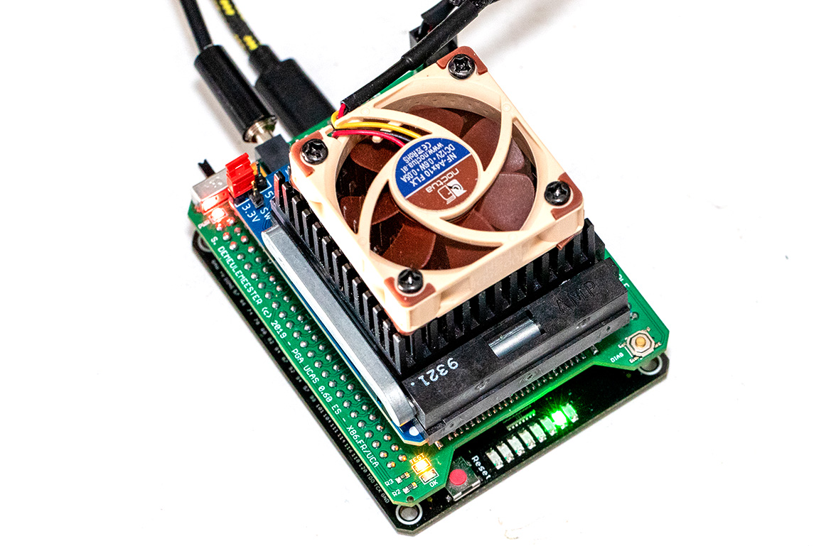
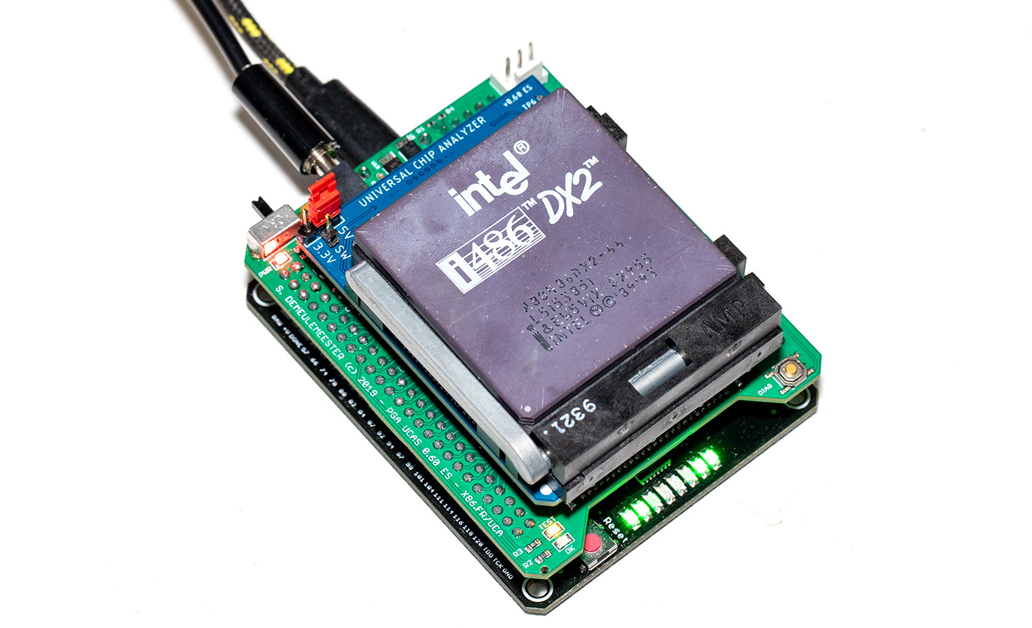
- The second (middle) layer is the heart of the Universal Chip Analyzer. It integrated all the bus transceivers, an internal management bus, and a much more advanced power delivery stage for the CPU under test. Bus transceivers can handle up to a 32-bit bus. The internal management bus can create interconnections between all the components (MCU, FPGA, etc.) spread on the 3 PCB layers. It’s used to bypass the FPGA for some later adapters and to support some nice features out of the box like adapters with embedded displays. The most interesting part is the power stage. The first iAPX86 UCA Shield was powered by USB only. It’s not possible anymore because advanced CPUs sometimes require lower voltages (+3.3V, +3.45V or +3.6V) and much higher current. A DC-DC converter is now integrated, along with a precision current/voltage monitor circuit that is also able to act as a programmable fuse. The voltage converter can be set externally to 5V or 3.3V, but it can also be set by the UCA software to any voltage from 2.2V to 5.5V by 50 mV step! I also added a standard 3-pin fan connector. Mandatory to keep some CPU like 486 DX4s cool! PS : The final PCB color will be black. The green one is cheaper and faster for prototypes…
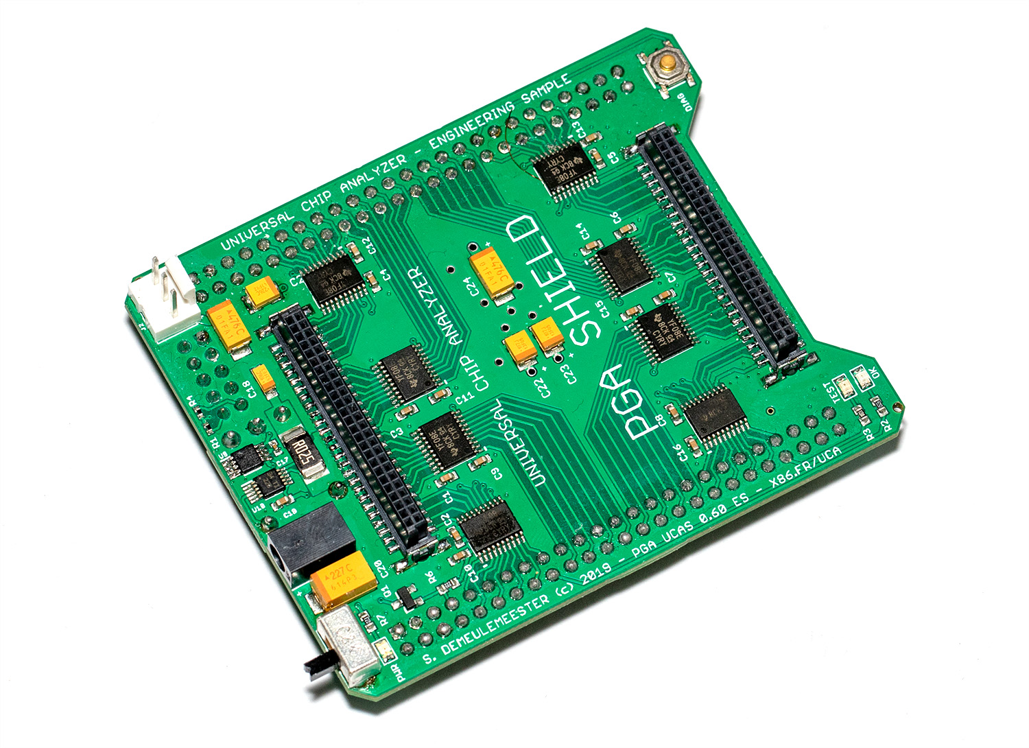
- The third (top) layer is a simple passive adapter with just two 50-pin connectors and a Socket (standard or ZIF) to accommodate the CPU under test. The UCA auto-detects the correct FPGA firmware to load according to the adapter plugged (except for later adapters able to support more than one CPU family). A jumper is often present to set a fixed voltage (usually 5V) or to select a software-defined voltage.

This hardware platform was designed for many upcoming adapters and should not evolve any further. It allows a much faster development of adapters, both in hardware and in FPGA HDL code. Many of them are already in development – some almost finished – and they will be released throughout 2020. Some very cool adapters are planned and yes, even for non-CPU!

* Now with i486 support (and soon much more)
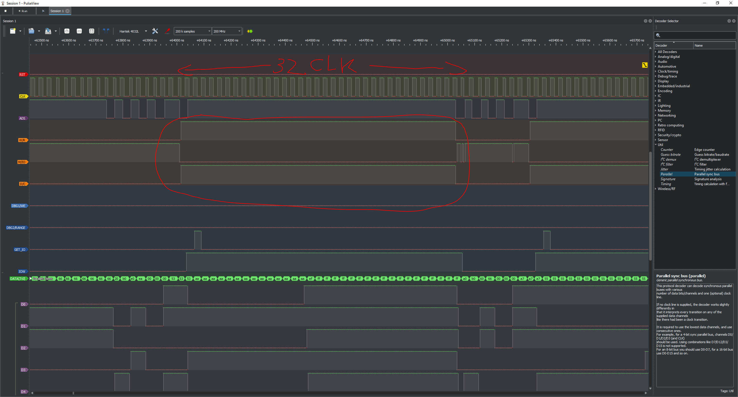
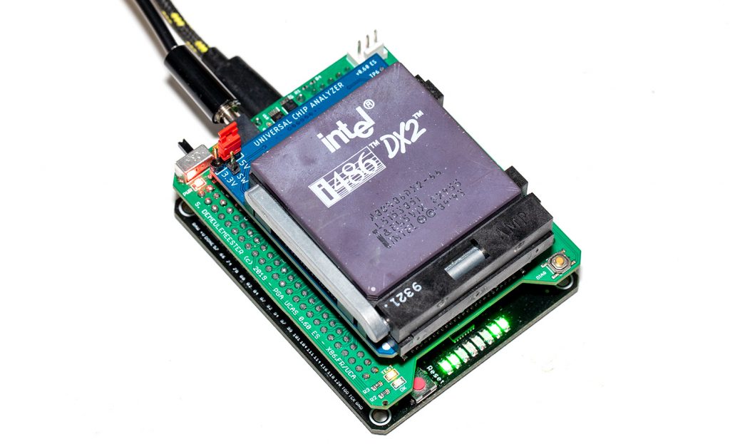
I started the development of this base platform with the fastest CPU with a 32-bit bus in mind: the clock-tripled 486 DX4. Because who can do more can do less. If the platform – and especially the FPGA – can support the DX4, it can also support every CPUs down to the 4004. That was a giant step versus the Intel 8086, the fastest CPU supported on the first iAPX86 shield. The 486DX4 is much more advanced, way faster and much more complex to interface. Tricks like forcing a stripped-down bus to 16 bit or adding wait states were forbidden.
Right now, the UCA supports any Intel 486 SX, DX, DX2 and DX4 CPU, from early engineering sample to QFP-on-adapter to late DX4s with write-back cache. The UCA is also able to set different bus frequencies, from 16 MHz to 40 MHz, with CPU frequencies up to 120 MHz (Intel 486 DX4-100 overlocked with a 40 MHz FSB).
 At this time, you probably wonder: what about the only 486-class CPU with a 50 MHz bus, the 486 DX-50? Well, it works fine at 40 MHz, but after many weeks, I’m now sure the UCA platform will not be able to support a “true” 50 MHz FSB. That’s just too close to the limitation of the bus transceivers I use. That doesn’t mean the UCA will never support a 486 DX-50 running at 50 MHz (or even higher), that only mean it will not support it without wait states. Back in the day, I don’t think there was a single 486 DX-50 based computer without wait states. When released, this specific CPU was well-known for its instabilities and manufacturers had to add (many) wait states to make it work properly.
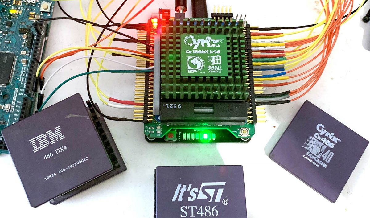
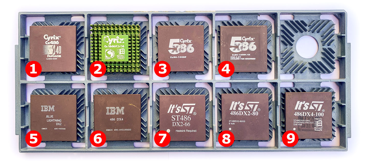
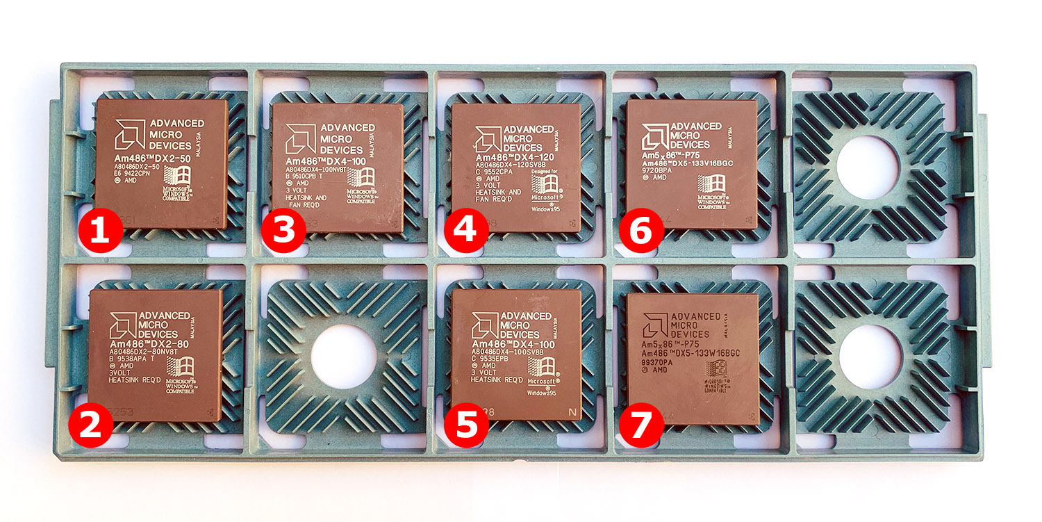
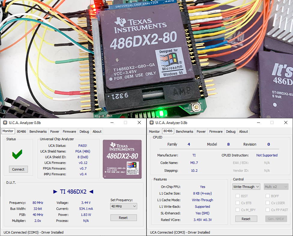
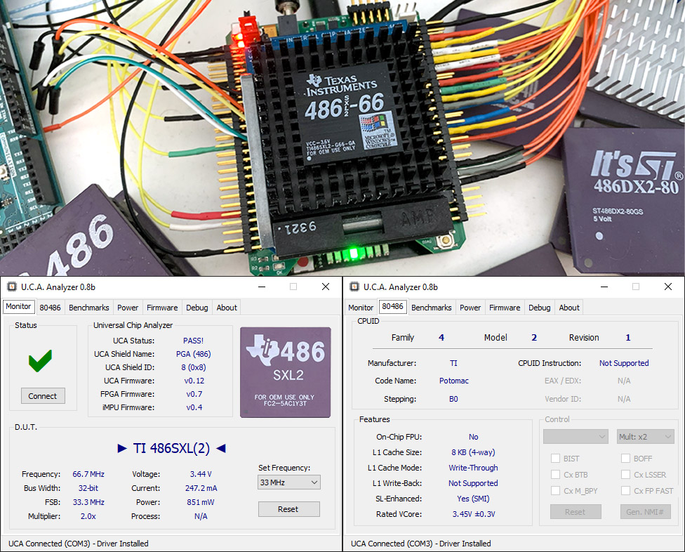
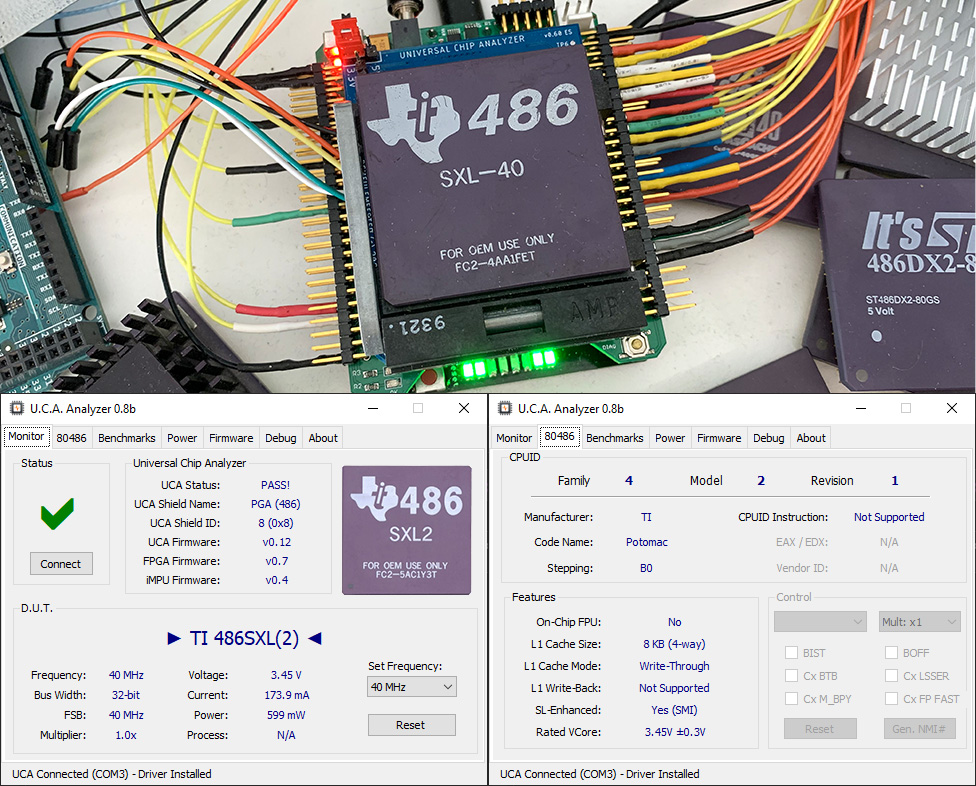
Now it’s time to talk about non-Intel 486s. The hardest part was to build an adapter able to support all the different 486 manufacturers out of the box (from AMD to Texas Instrument to Cyrix) without any dip switches despite the different pinout they use. I’m confident I now found the perfect hardware tricks and, even if they’re not working right now due to lack of software implementation, the 486 Adapter for the UCA will support (very) soon all 486s. Yes, that includes AMD & Cyrix 5×86, and some outsiders like UMC 486s and the elusive Texas Instrument 486 SXL2-66!
* Now Truly an Analyzer
I always wanted the UCA to be a true Analyzer (and not just a tester), able to dig into the microarchitecture by allowing the user to mess with internal registers and CPU pins. The path is quite complex because the data has to be transferred between several layer. The FPGA is directly connected to the CPU under test and loaded with custom HDL code (the “FPGA Firmware”). A microcontroller IP is inferred inside the FPGA and internally connected to various control signals, to the main RAM used by the CPU, and also to the external microcontroller of the base board. Some C code, written with the Xilinx SDK, is executed by this internal MCU to handle the communication between the FPGA parts and the external MCU. I call it the “iMPU Firmware”. More C code is needed on the external MCU (for the ATMega32u4, called “UCA Firmware”) to pass the data to the USB connector. Finally, a Windows 10 software program written in C# to communicate with the UCA.
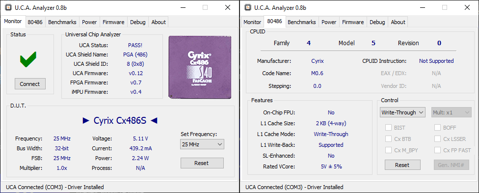
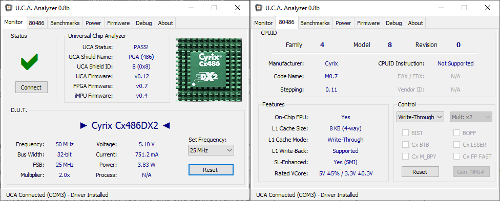
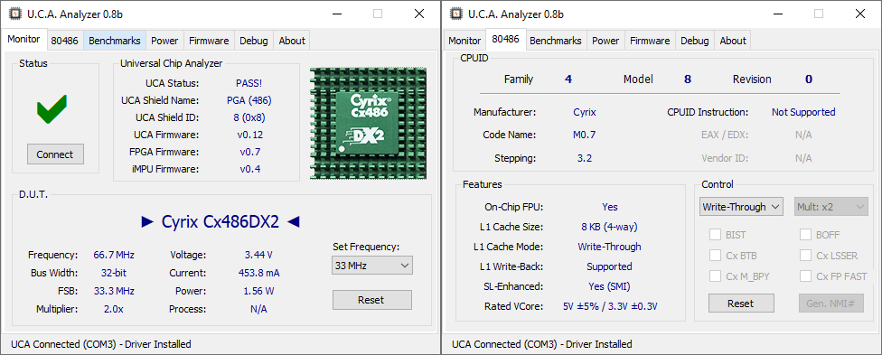
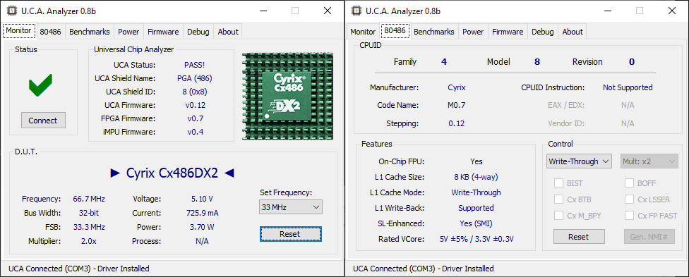
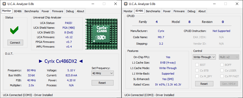
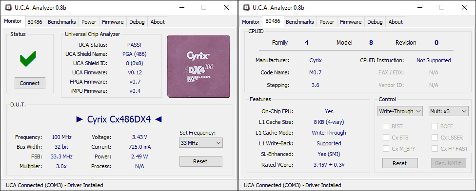
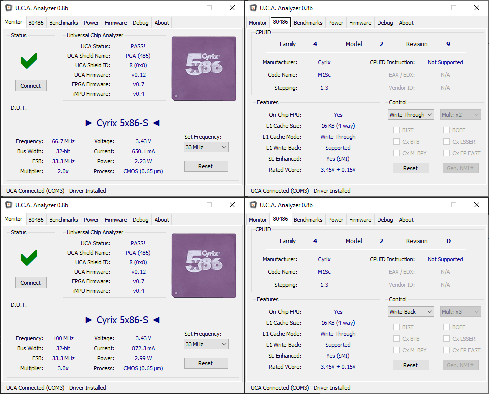
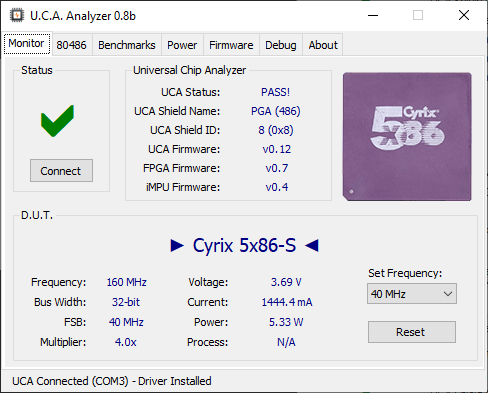
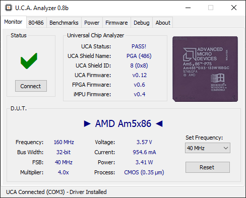
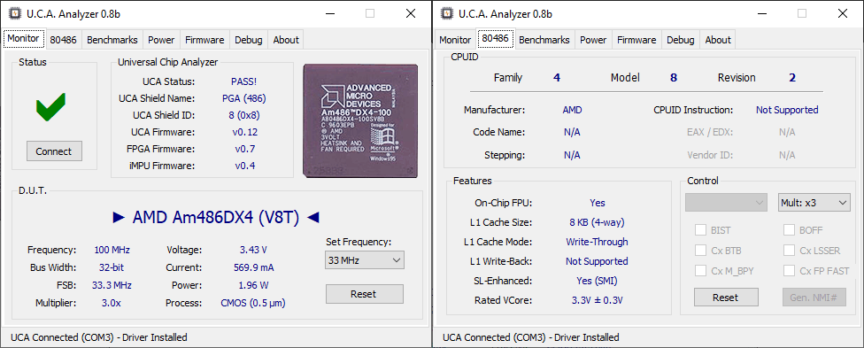
Here is the actual UCA Analyzer tool, running with an Intel 486 DX4-100 overclocked to 120 MHz.
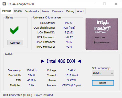 On the main tab: the testing status (INT or FP Test in progress, Pass, etc.), various version information on the internal firmware of the UCA, the actual CPU under test detected with actual CPU & FSB frequency, multiplier, voltage, current, power and process. You can also select a different frequency and reset the CPU.
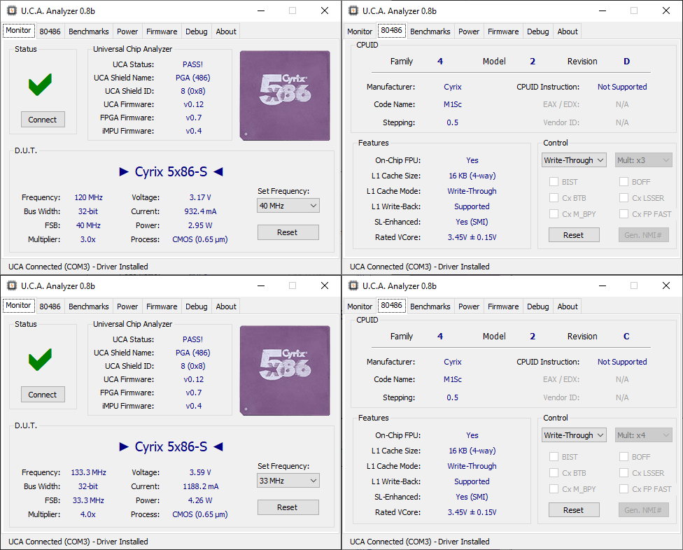
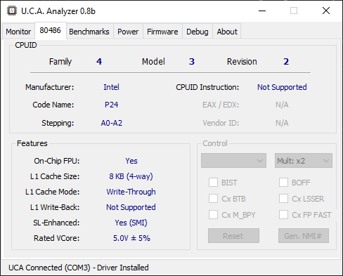
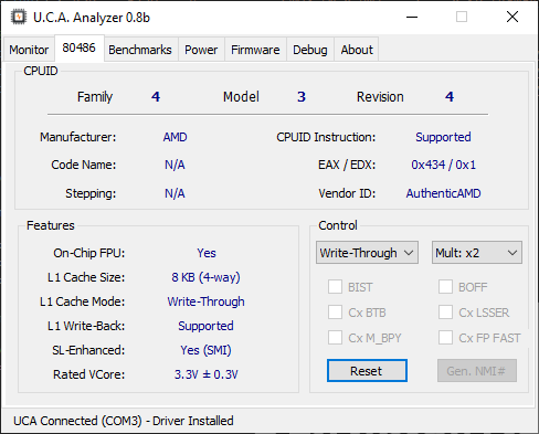
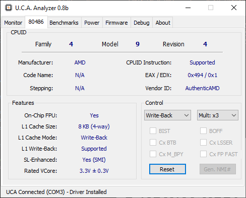
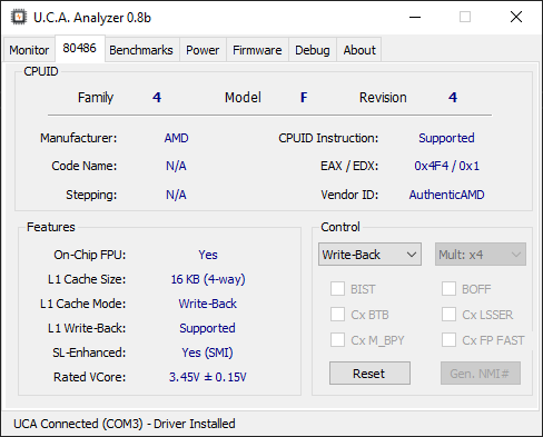
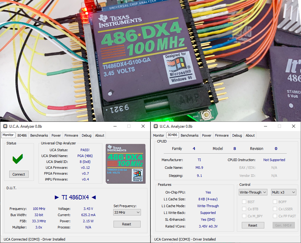
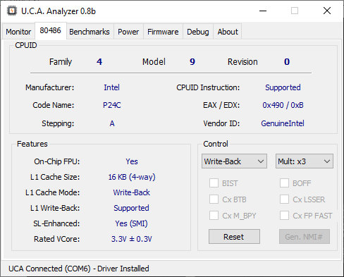 On the specific 486 tab, the actual CPUID of the CPU (acquired from the CPUID instruction or at reset if CPUID instruction is not supported), various information on supported/enabled features and a work-in-progress “control” section to assert some pins of the CPU. For example, we have an Intel 486 DX4-100 in Write-Back mode with CPUID 0x490. If you set the cache to Write-Through mode, the CPUID for this CPU changes to 0x483. Many new features are planned here.
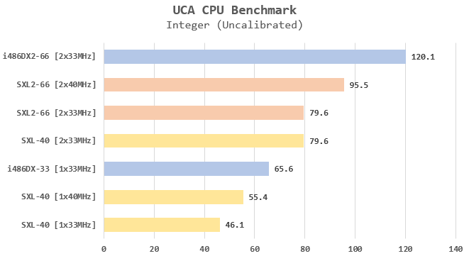
 Another work-in-progress tab is for a benchmark feature. The values displayed are random for now, but everything is already implemented to support INT & FP benchmark. The goal is very different than traditional benchmark. Here, we will focus on microarchitecture benchmark only. There are absolutely no bottlenecks usually found on a “real-world” motherboard like chipset or EDO/FPM RAM. The UCA is able to feed the CPU with 0 wait states, so all data is read/written immediately, as if they were in cache. The true power of the internal ALU/FPU, at their maximum process capabilities, can be revealed. More about the benchmark mode later.
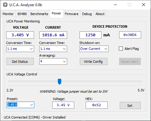 The “Power” tab is one of the most significant improvements. On the top block, you can precisely monitor the voltage and current needed by the CPU, but also configure the internal ADCs (averaging & conversion time) and set the type and value of the protection (usually overcurrent). You can also reset the Alert Flag when shutdown due to overcurrent happens. On the bottom block, you can set the actual voltage for the CPU under test, from 2.2V to 5.5V by 50 mV increments. Useful to test undervoltage or overclocking. Ie: the 486 DX4-100 I used for the screenshot doesn’t work at 120 MHz at 3.3V but everything is fine at 3.45V.
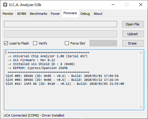 The original Mojo v3 comes with a 60+ MB FPGA bitfile (firmware) uploader written in Java. I adapted it to handle many different bitfile “slots”, but it was time to rewrite it from scratch. I integrated the FPGA firmware uploader tool to the UCA analyzer, with the same features. You can still check all installed bitfile, slot by slot, and upload/delete them as needed. Now with a tool less than 1 MB and without Java.
 The “Debug” tab logs all sent/received communication for debugging purpose. I also added a feature on the last “About” tab to easily upload the base UCA firmware (for the external microcontroller).
* Soon truly on sale everywhere?
Many CPU collectors or retro-enthusiasts already expressed their interest for the universal shield described above. A beta-testing phase will begin soon, starting with the 486 Adapter then with many others. I’m still wondering if it’s better to sell the adapters one by one, as soon as they’re ready, or to wait until at least 3 or 4 are available. The latter option can help keep costs as low as possible by panelizing the adapters. The final “retail” price for the UCA (base FPGA board + Universal Shield, without top adapter) is expected to be around $150. Adapters cost will be around $50 or less, depending of the Socket included. Finding ZIF PGA sockets at decent price is the most challenging part, especially for CPUs like the 286s. All those who have already bought an UCA with the iAPX 86 Shield can reuse the FPGA board with a firmware update, so they can expect a big rebate.
Progress is going to be fast, so stay tuned for more exciting information and in-depth CPU analysis!
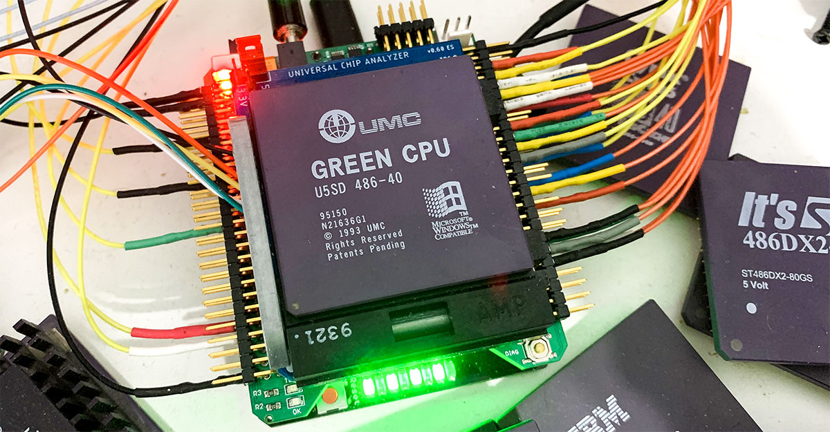
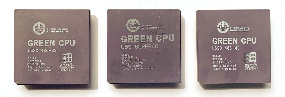 The most common one was the U5SX (sometimes marked U5S) clocked at 25, 33 or 40 MHz and without FPU. Some UMC Green CPUs labeled “U5SD” were also released. Contrary to what you might think, they don’t include a FPU – verified with the UCA – but are just supposed to use the “DX pinout”. The meaning of this mention is unclear because both the i486SX and the i486DX shares the same layout for non-FPU related pins. Some guys have claimed that the difference is a relocation of the NMI pin, but I have not noticed that. UMC also released extremely rare U5D (with FPU) and U486DX2 (clock doubled with FPU), but only a couple samples are known today worldwide.
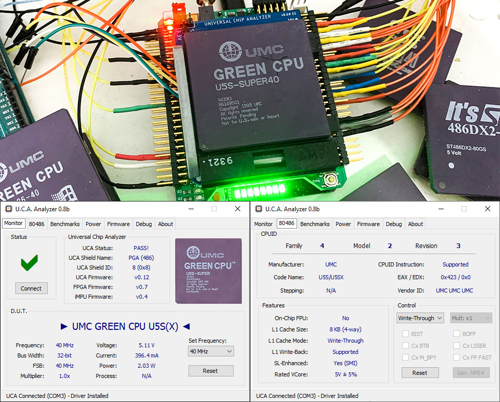 The Universal Chip Analyzer is able to test all UMC 486s, even if I still have an issue at 33 MHz and 40 MHz to grab every I/O. Code fetch works fine, but the output on I/O ports are sometimes dropped. It’s probably easy to solve, but I really need a copy of the UMC 486 manual / datasheet. Unfortunately, it seems nobody has one in the CPU collector’s community. If you can help, you’re more than welcome!
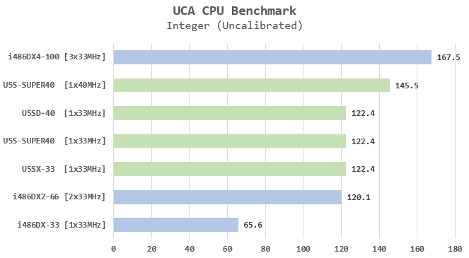 As you can see, all UMC CPUs (U5S-SUPER, U5SX and U5SD) offer the exact same results when clocked at the same frequency. You also probably noticed the awesome relative performance of the UMC 486 versus the Intel 486s. Clocked at 33 MHz, the UMC 486 is as fast as an Intel 486DX2-66 and, when clocked at 40 MHz, it’s almost as fast as an Intel DX4-75. That’s not a bug. The UCA doesn’t have any wait-state on memory subsystem and actually uses a mix of heavy Integer divide and multiplication instructions for the benchmark. This result comes from the ultra-fast ALU designed by UMC, especially on divides. While Intel 486s requires 40 cycles to perform a INT divide, UMC 486s only need 7 cycles. That’s more than 5 times faster! However, in real-world applications, the UMC 486-SUPER at 40 MHz was on par with an Intel i486SX2-66. Still excellent!
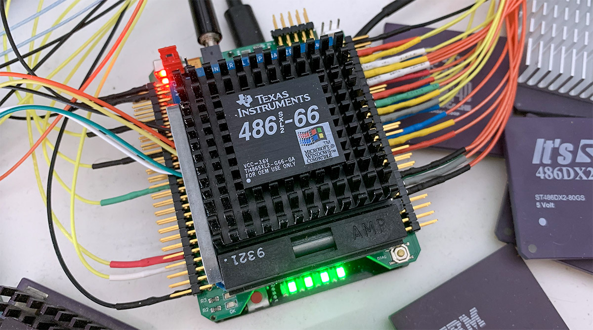
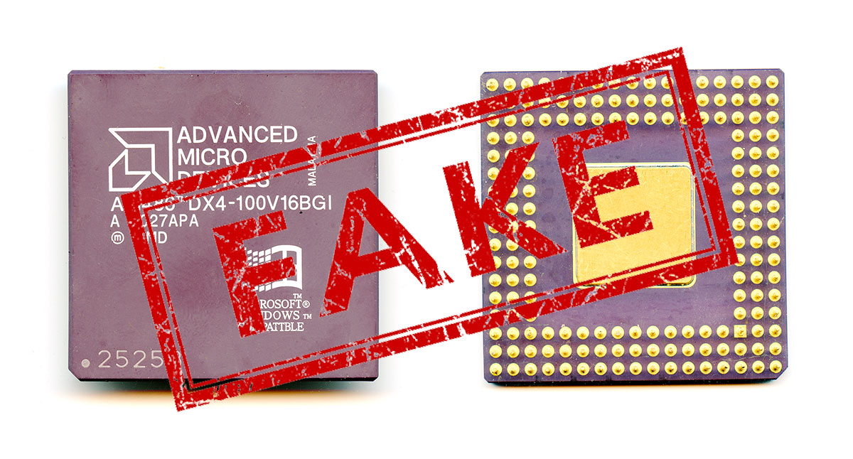
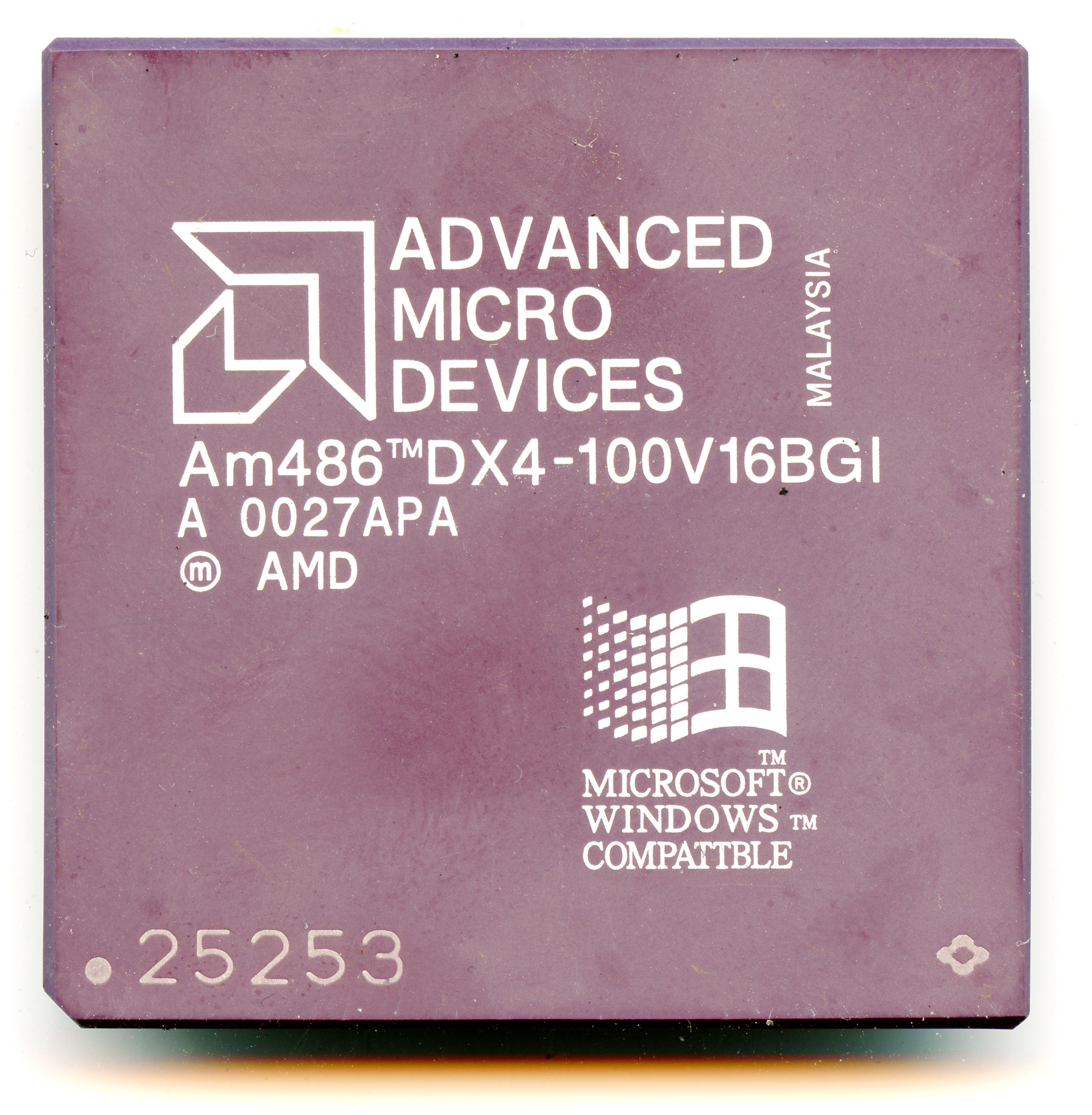
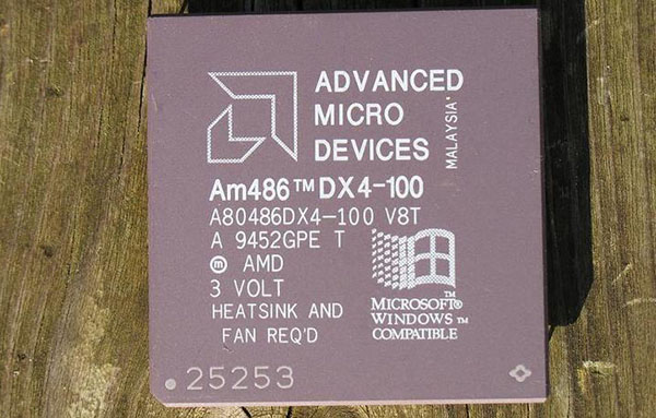
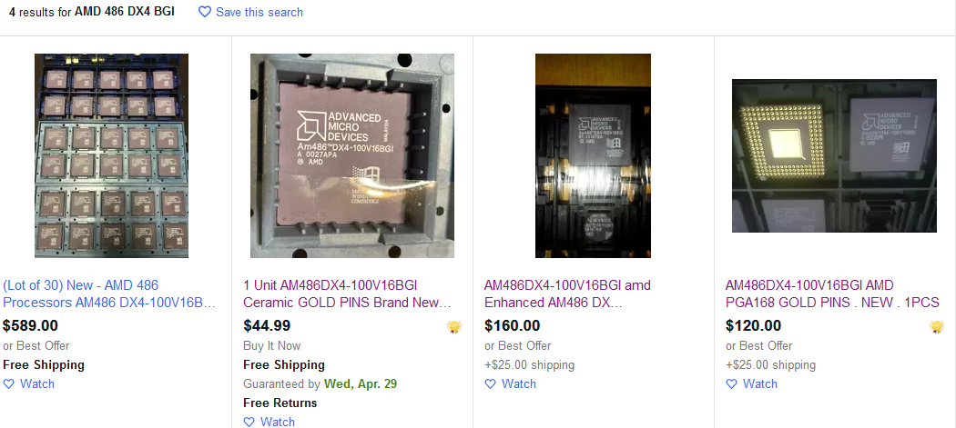
 There is no doubt at this point that this CPU is a counterfeit Am486DX4. The only question remaining is when was it remarked by fakers? Counterfeits CPUs – especially 486s – were common in the 90s to boost frequency, but here, the original CPU was already an Am486DX4-100 (albeit a very early one with 8 KB L1 Write-Though Cache, instead of the expected 16 KB L1 Write-Back Cache). More recently, in the mid-2010s, old CPUs from the 90s were also faked to target CPU collectors all over the world.