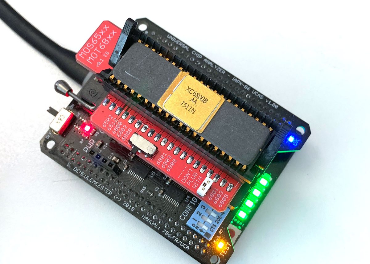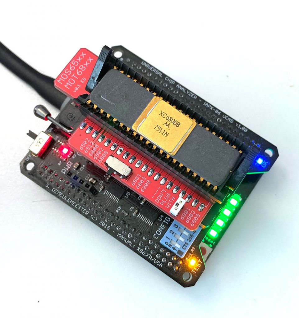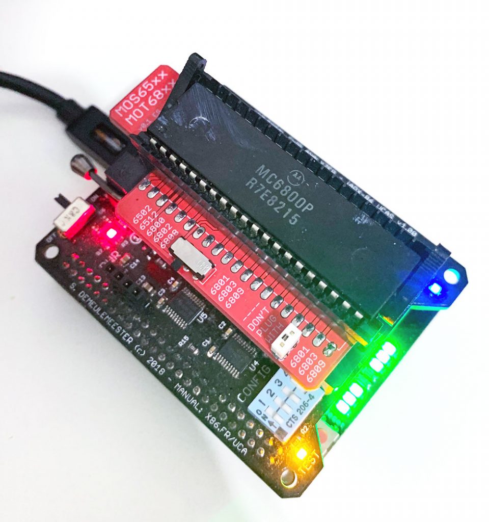
While adding support for the Motorola 6800 on the Universal Chip Analyzer, I remembered the famous HCF instruction supposed to be present on that CPU. The Half & Catch Fire opcode is an undocumented and semi-mythical machine instructions with destructive side-effects, supposedly included for test purposes on several well-known architectures going as far back as the IBM System/360. The Motorola 6800 was the first – and almost only one – to have a HCF instruction well-known by the developers back in the 70s. It doesn’t really destroy the CPU, but makes it switch into a kind of debugging mode. Allegedly, HCF instruction on the 6800 should toggle the address lines in order very quickly. Legend added: up to the point that some support component might catch fire!
I read many resources online, including the Wikipedia page, about the HCF opcode and I found many contradictory information. It seems very few people actually tested the 6800’s behavior by themselves. Good news: the UCA has been created for this kind of experiment!
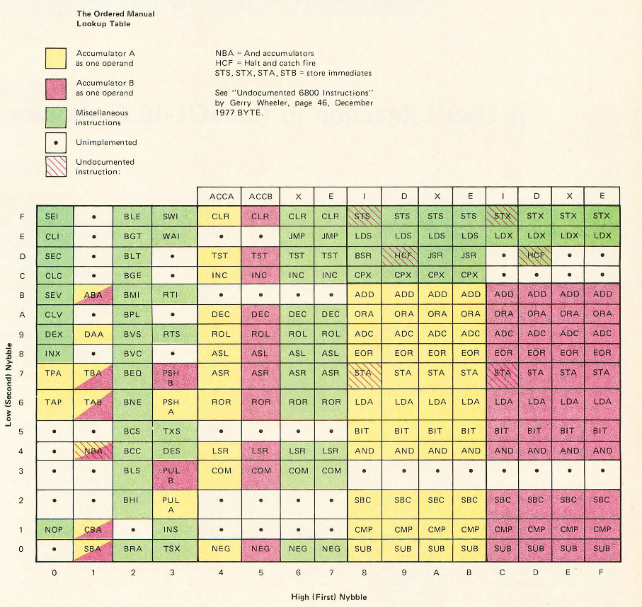
According to Wikipedia, the HCF opcode is 0x9D and 0xDD. I also found some other source locating it at 0x14, 0x15 or 0xCD, like on this Motorola 6809 and Hitachi 6309 Programmer’s Reference.
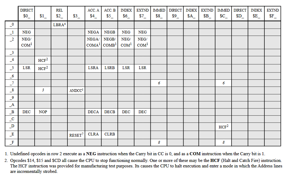
And here is another (different!) opcode matrix from here :
I have also investigated some other undocumented opcode (0xBD, 0xEB, 0xFB). All tests has been done on a Motorola MC6800P with a 1 MHz clock.
-
0x14 / 0x15
Inserting 0x15 opcode doesn’t seem to have any effect on the CPU at all. Both opcode seems to be treated as NOPs, wasting 2 machine cycles. Registers unchanged. 0x14 executes a AND between both accumulator (A & B) and stores the result in A. However, only the later MC6800P seems to support this. An early XC6800 prototype does not to fetch the 0x14 opcode correctly.
-
0xCD / 0xED
Both instructions crash the 6800 and make it unable to execute any more code until a full RESET is triggered. Exactly 64 ms after the opcode has been fetched, the CPU starts to toggle address line almost in order, but with many glitches and only for A0-A6. A7-A15 remain erratic.
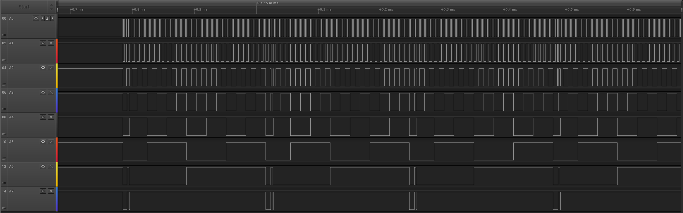
But more interesting, I noticed a strange behavior on the upper address line. The 5 upper address line (A15-A11) started to count in reverse order from 0b11111 to 0b00000 at a very slow, human-readable, rate :
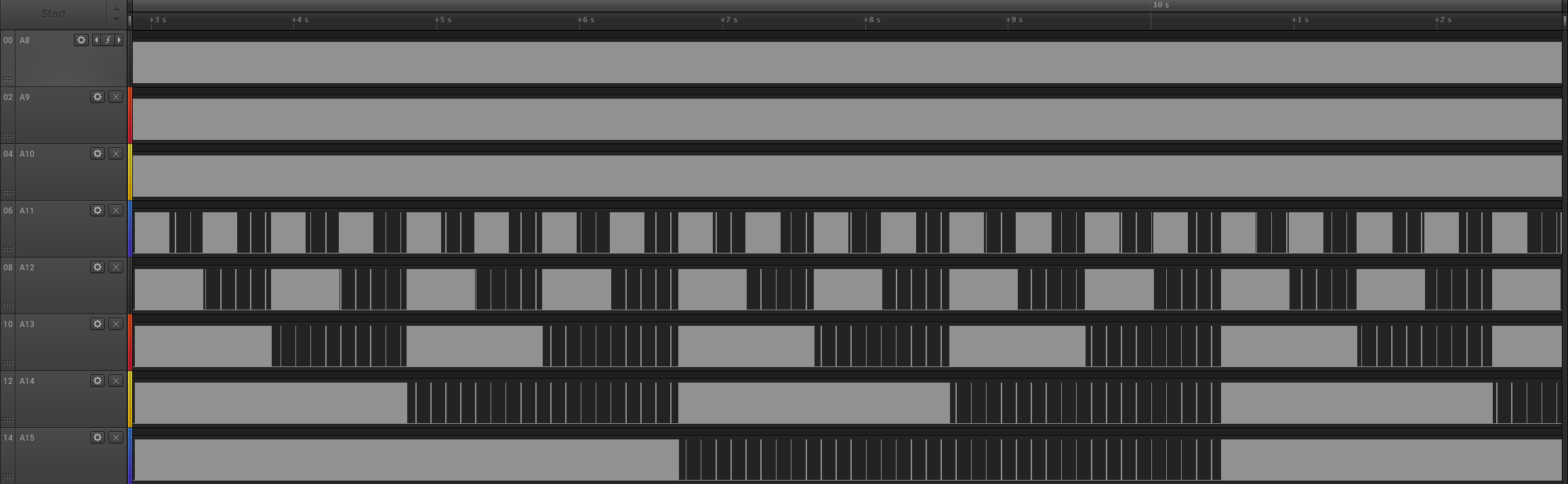
The whole process (similar with both instruction) takes ~8 seconds with the 0xCD opcode and much longer (~60 seconds) with the 0xED opcode. Has this been added for simple human debugging (without oscilloscope or logic analyzer, costly in the 70s), or is it just a glitch? Hard to tell.
-
0x9D / 0xDD
Here we find the expected “HCF” debug instructions. 64 ms after being fetched (which is quite long), the CPU starts to toggle all address lines in order, very fast (500 kHz for a 1 MHz clock) and with a clean square wave.
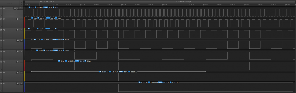
After the HCF has been fetched, the 6800 stops responding to interrupts. A hard RESET is the only way to resume operations.
-
0xFD
While messing with invalid opcode, I found another HCF instruction on the 6800. This one seems to behave exactly like the 0x9D/0xDD HCF, but is twice slower : 250 kHz instead of 500 kHz.
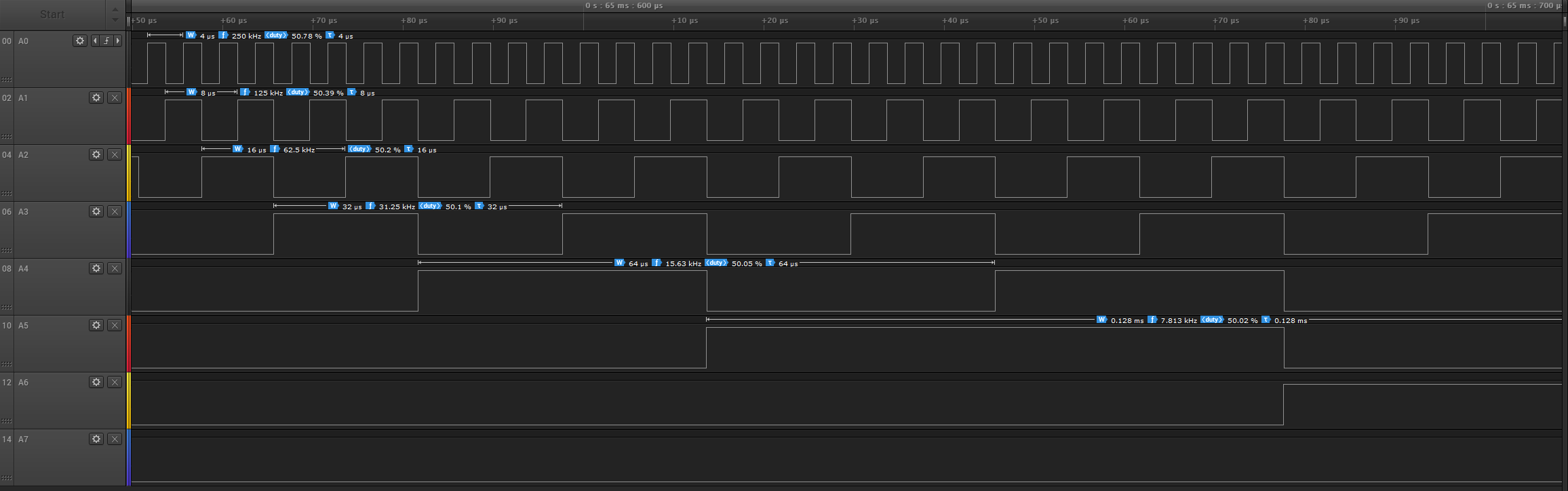
It seems 0x9D/0xCD/0xDD/0xED/0xFD are all related to HCF, but only 0x9D, 0xDD and 0xFD produce a clean (glitch-free) output.