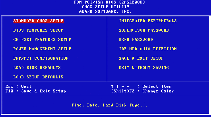
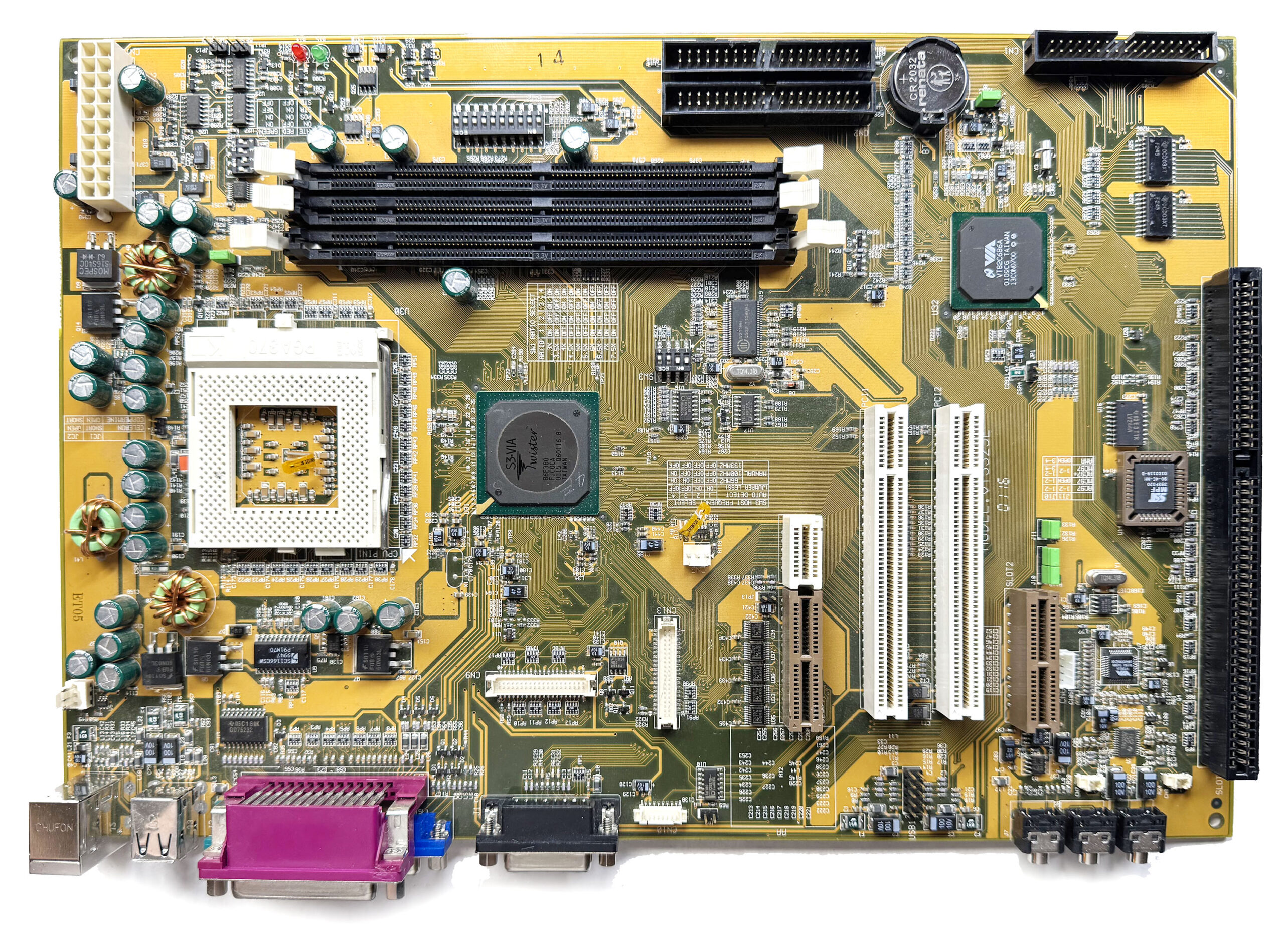
The next board from the cemetery is the VT5329E, a Socket 370 development board which was probably used to validate the switch between Trident to S3 Integrated graphics in early 2000s. Unlike reference boards, which are intended to serve as the basis for commercial motherboards, development boards are primarily designed for R&D purposes. Its unusual form factor leaves little doubt that the VT5329E is one of them.
The is significantly larger than a standard motherboard and will not fit in a conventional ATX case. This is confirmed by the unusual placement of the audio jacks, which are aligned with the PCI slots and would prevent the board from being mounted properly. The board has 3x SDRAM, 2x PCI, 1x ISA and 1x AMR slots, and is based on the VT8603 (“Twister”) Northbridge, the first VIA Northbridge to use a S3 integrated chipset instead of the previous Trident IGP.
Between 1998 and 2002, VIA’s Socket 370 chipset lineup became rather confusing, with numerous renamings and rebrandings over that five-year period. All VIA Socket 370 IGP northbridges internally use the VIA Apollo Pro 133, or Apollo Pro 133A, northbridge combined with a third-party graphics core. As a reminder, the main difference between the Apollo Pro 133 (VT82C693A) and the later Apollo Pro 133A (VT82C694X) is that the latter adds support for AGP 4X. Both supports FSB 66/100/133 and SDRAM PC133.
Let’s try to summarize everything here.
VT8601 (Apollo PLE133) – The original Socket 370 IGP from VIA. Originally named “Apollo ProMedia”, then “Apollo PM601” and finally “Apollo PLE133”, its final commercial name. Based on the Apollo Pro 133 (not-A), internally connected using AGP 2X to a Trident Blade3D Graphic core. It was officially named “VT8601A” later.
VT8602 (Apollo PLE133T) – A later revision of the VT8601, based on the Apollo Pro 133A with support for AGP 4X to connect the same Trident Blade 3D Core. This Northbridge is also named “VT8601T” because it supports Intel Tualatin CPUs.
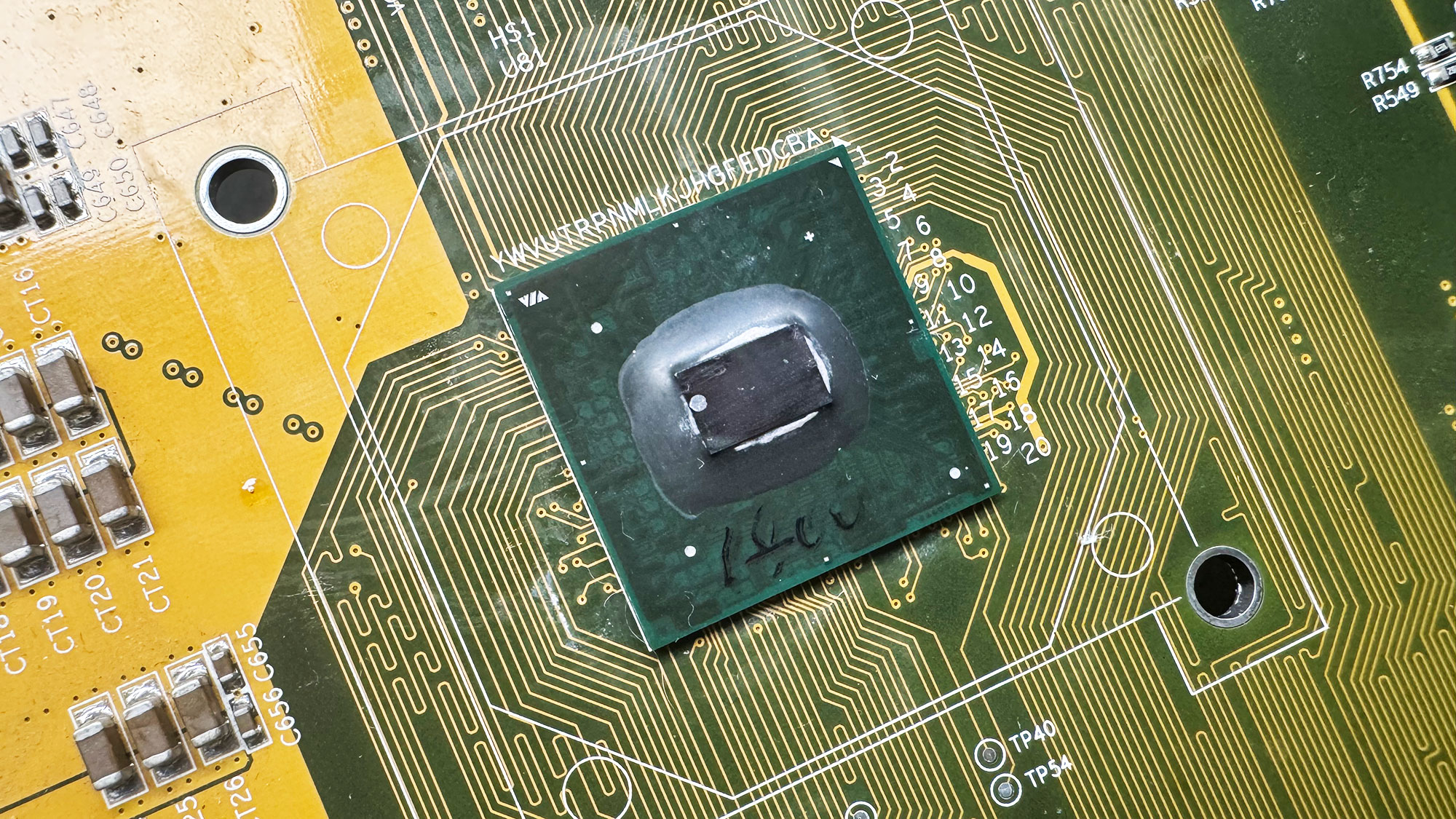
VT8603 (ProSavage PN133) – Based on the Apollo Pro133A with a S3 Savage4 3D architecture (named “Twister” by S3). This Northbridge has been designed as a Mobile part, with additional features like direct support for LCD panels or more advanced power-saving capabilities. It doesn’t support an external AGP slot. That’s the Northbridge on the VT5329E Development board. VIA used the contraction between “Apollo Pro” and “Savage4” to finally name it “ProSavage”.
VT8604 (ProSavage PL133/T) – A stripped-down version of the VT8603, with Mobile-specific features removed and still no support for an external AGP slot (IGP is the only option for graphics). It was designed as a cheaper option for the Value Desktop segment.
VT8605 (ProSavage PM133) – This part is a “high-end” Desktop part with IGP, almost identical to the previous one, but with support for an external AGP 4X slot. Basically, an Apollo Pro 133A with a embedded electrical switch between the internal S3 IGP and an external AGP 4X slot.
VT8606 (ProSavage PN133T) – A minor revision of the VT8603 with support for Intel Tualatin (CPUs). This Norhtbridge is quite rare and has been used exclusively in embedded computers, SFFs (like early Shuttle barebone) and some elusive laptops. It has been produced up to the early 2010s.
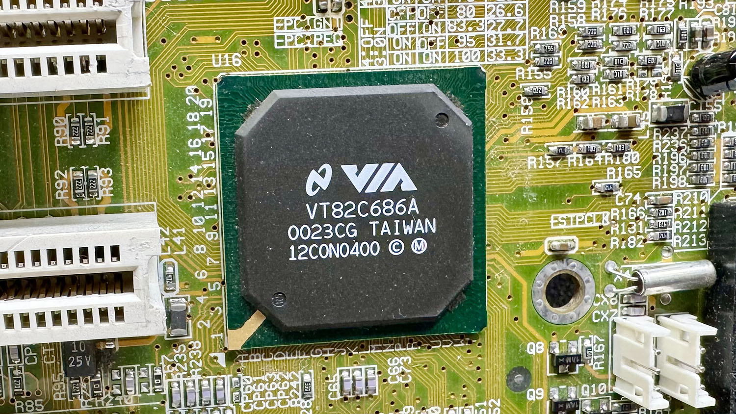
All these Northbridge are usually accompanied by the VIA 686A or 686B Southbridge. As an early board, we have a VT82C686A on the VT5329E:
There are not many differences between the 686A and 686B. The latter basically just adds ATA100 (UDMA 5) support. Both supports PCI-to-ISA bridge, AC’97 audio, an integrated Super I/O chip with monitoring, SMBUS and USB 1.1 (up to 4x ports). On the VT5329E, it seems clear that the audio codec part was specifically targeted for evaluation.
The board has jumpers for AC’97 (provided by a VT1611A), MC’97 (modem counterpart), AC’97+MC’97 and for the dedicated audio/modem codec slot (AMR). Note that this is the older (circa 1998) AMR specification and not the newer CNR standard that was introduced by Intel in 2000.A very interesting point is the strange slot located close to the Northbridge
Physically, it resembles an AMR slot with a small white extension similar to the end of a PCI slot. Electrically, however, it has nothing to do with AMR. Based on the PCB traces and the voltage translators located nearby, my best guess is that this slot breaks out the LCD panel signals for debugging purposes.
The VGA port on the VT5329E doesn’t work as expected. It outputs a strangely formatted signal resulting to a scrambled display. It may try to output a LCD panel signal. With an external PCI card, everything is ok
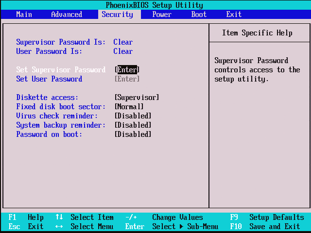
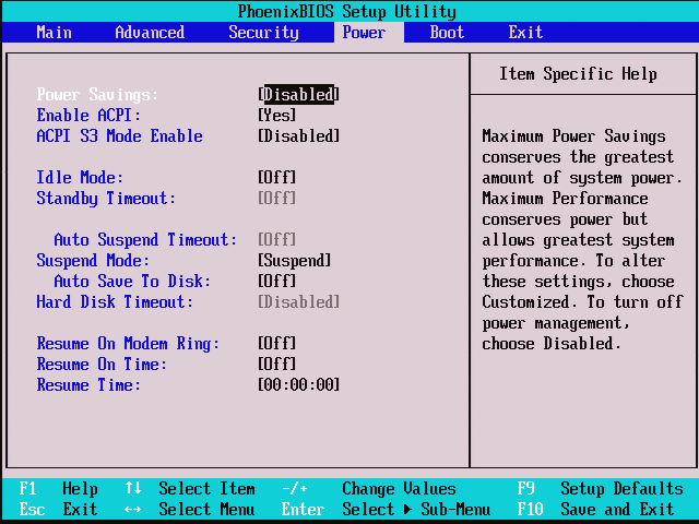
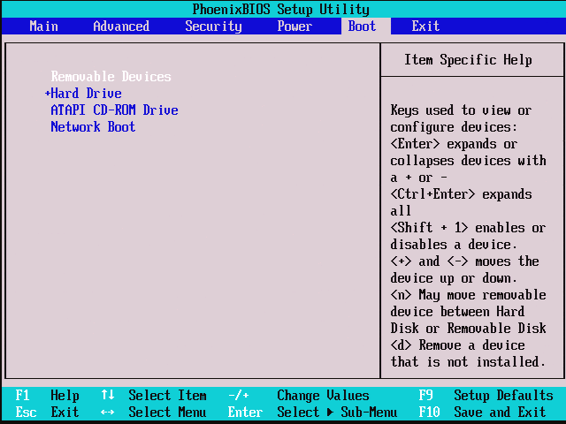
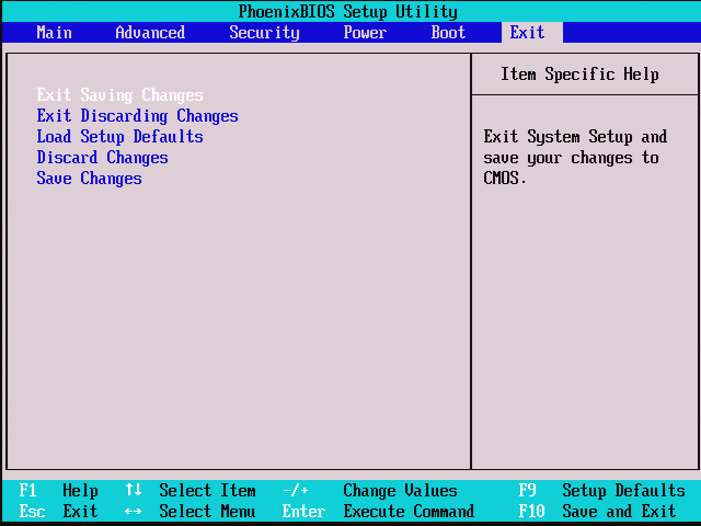
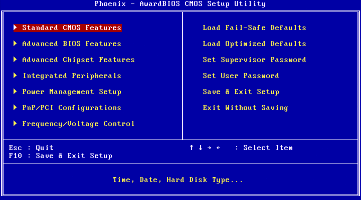
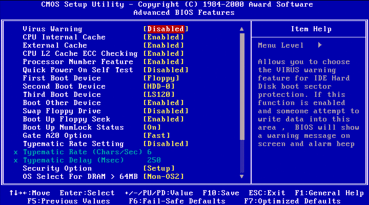
We are greeted by a Phoenix BIOS 4.0 instead of the usual Award 6.00 BIOS. Not really surprising for a Mobile development platform (Phoenix BIOS were much more common in laptop). The boot strings include “FOR EVALUATION ONLY. NOT FOR RESALE” and “VIA Twister (VT8603 + VIA686A) –12669r01.101” with a build date on 2001-05-16. The configuration menu is quite nice:
I would have liked to find other system based on VT8603 “Twister” or PN133 chipset, but I couldn’t find a single one. If you have any information about a computer using this Northbridge, just let me know in the comments, I’ll add it here!
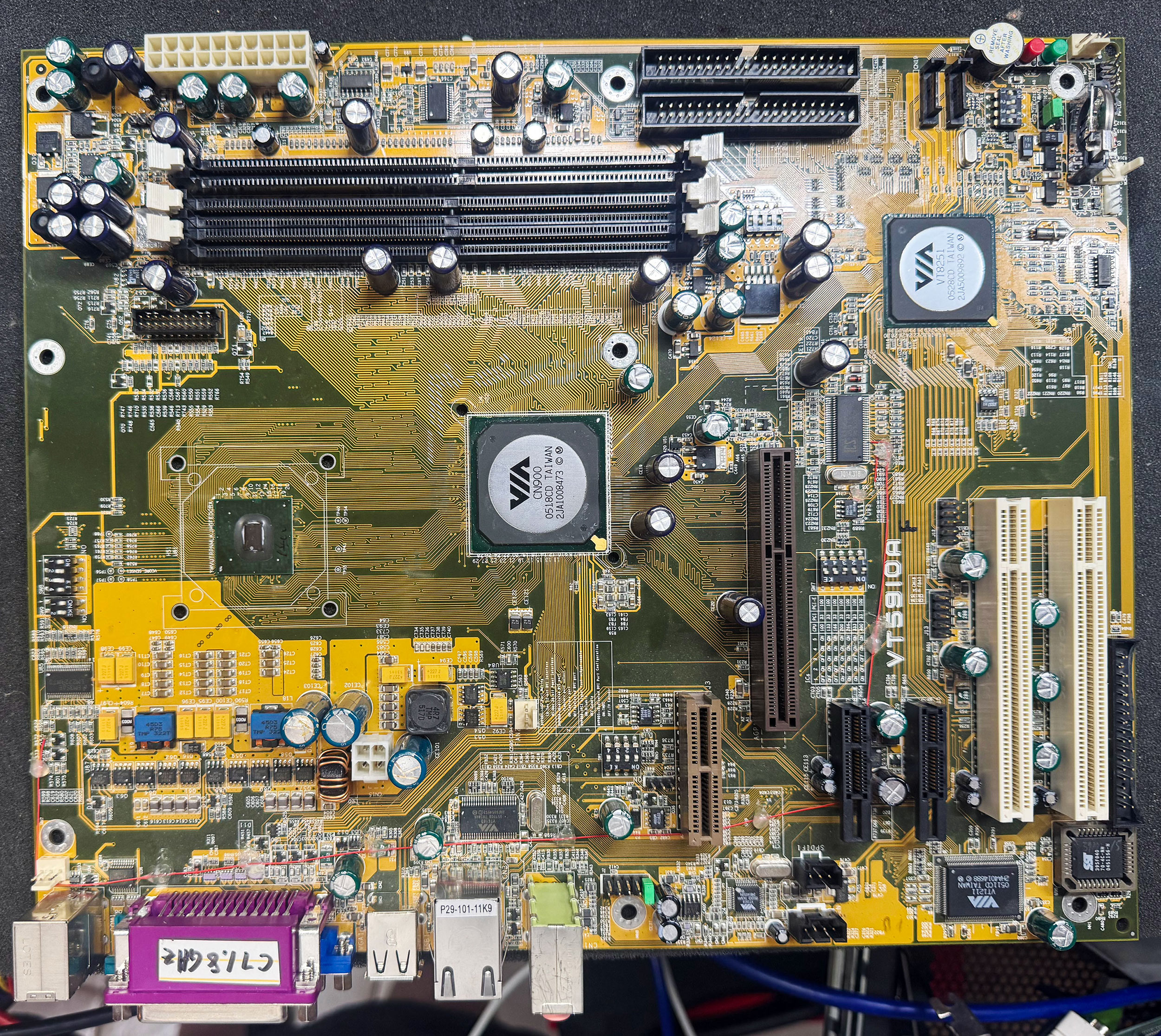
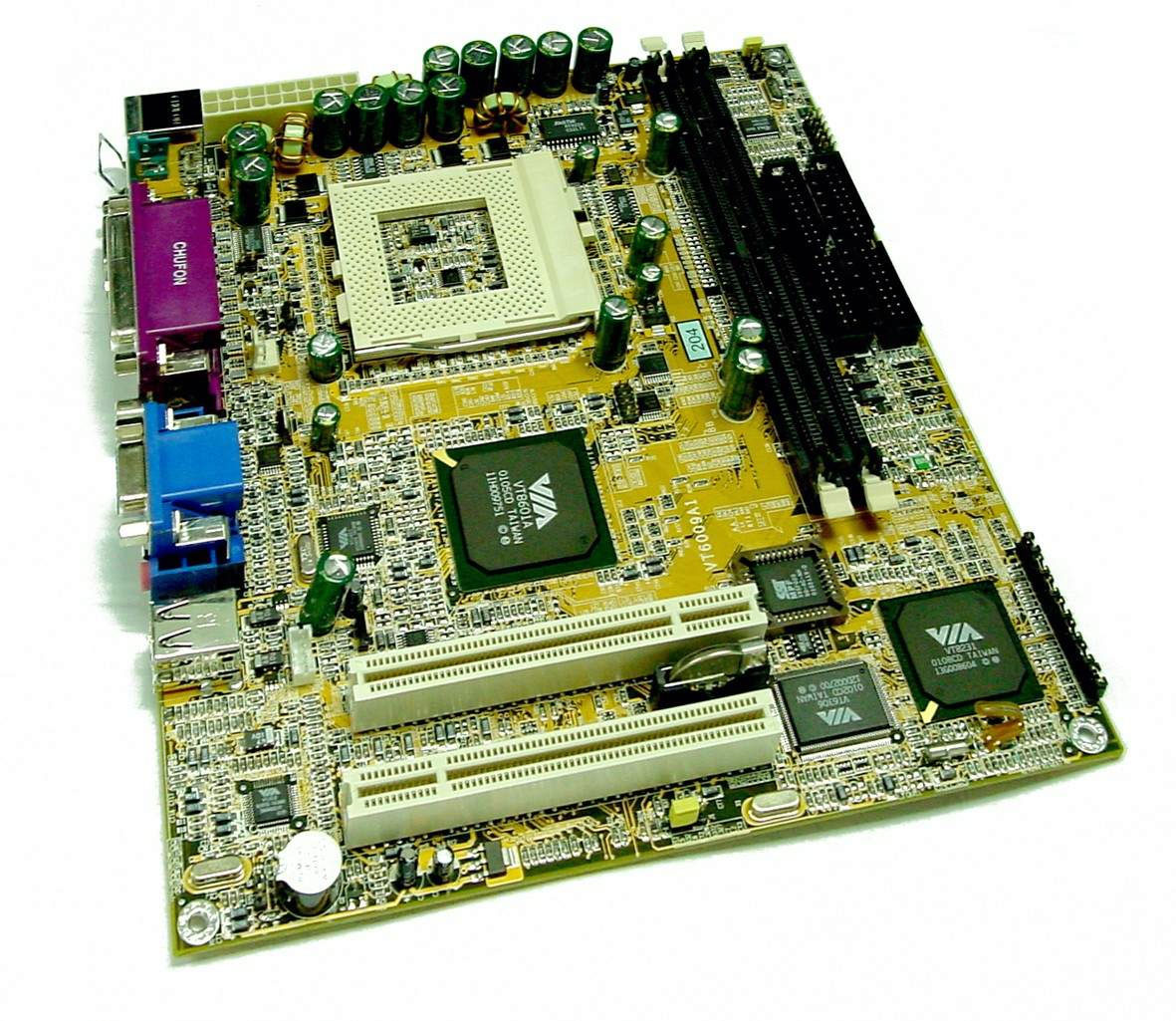
The VT5910A development board is one of the most interesting boards from the cemetery.
Unfortunately, I received it in fairly poor condition. All the heatsinks had been brutally torn off, there were scratches on both sides of the PCB, several connectors were damaged, pin headers were bent, some traces were cut, and thermal grease was spread everywhere. After some initial cleaning, this is what it looked like:
VIA VT5910A Development Board
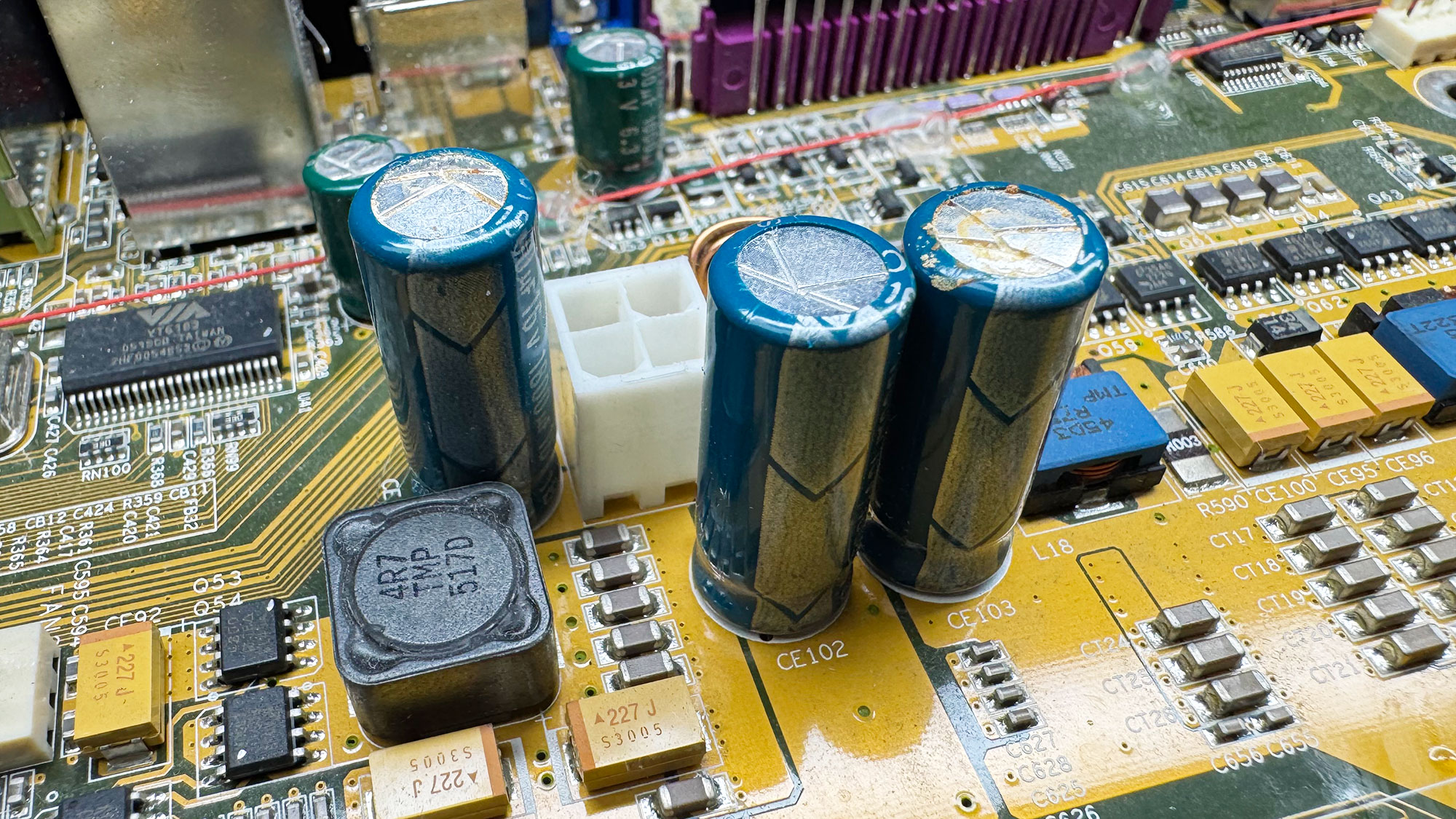
I repaired most of the damaged connectors and PCB traces, but the board still had 12 V shorted to ground somewhere. I eventually traced the short to one of the dead decoupling capacitors, which was visibly bulging and leaking.
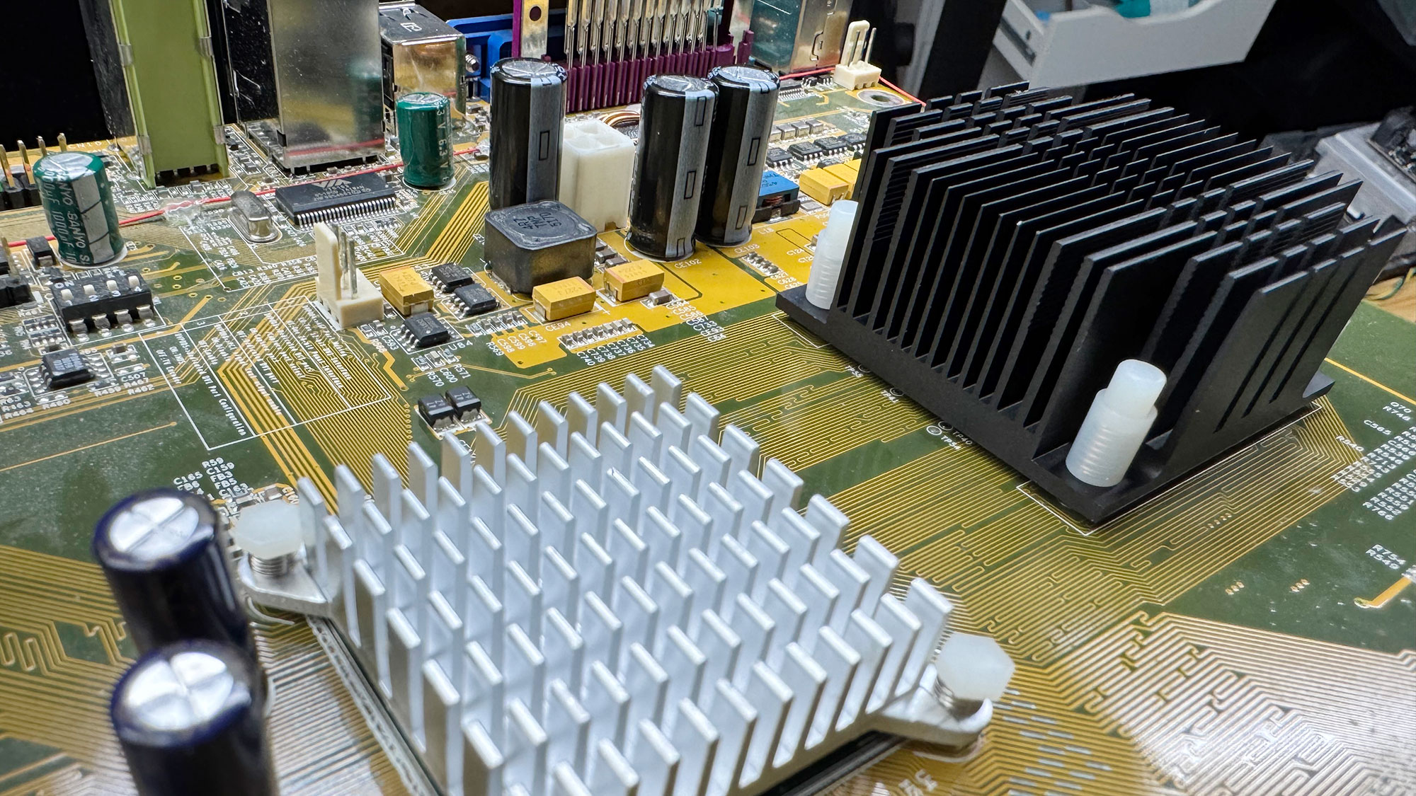
Original caps bulging and leakingReplaced capacitors and new heatsinks!
After replacing all the defective capacitors with brand-new Rubycon caps, I had to find suitable replacement heatsinks. The CPU cooler uses a 41 × 41 mm mounting-hole spacing, similar to the Pentium M reference cooler. I found a compatible one, reassembled everything with fresh thermal paste, powered the board on… and it booted!
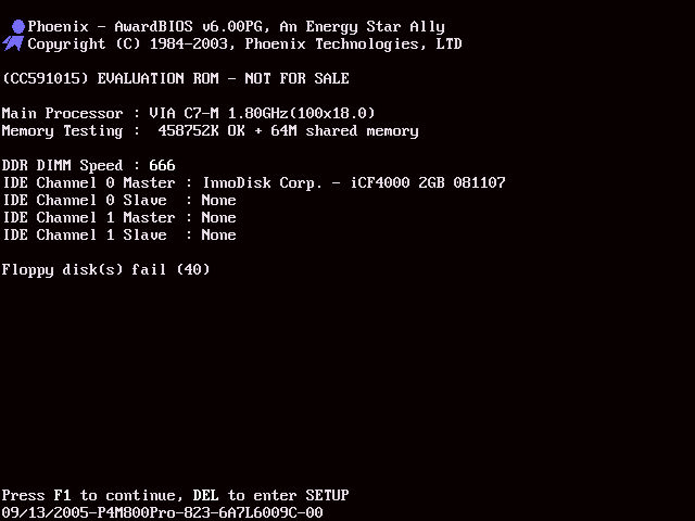
Now let’s take a closer look at what this board actually is. The VT5910A is a full-size ATX development board assembled in mid-2005, with many features that were still in an early stage at the time. The soldered engineering-sample CPU is a VIA C7-M clocked at 1.80 GHz, in a NanoBGA2 package, with CPUID 0x6A9. This processor had only just been announced, and mass availability would not come until the following year. My original C7 review on x86-secret.com was published in May 2006.
VIA C7-M 1.80 GHz Engineering Sample
The C7-M, based on the Esther (C5J) core, is a low-power x86 microprocessor family introduced by VIA in 2005 and designed by Centaur Technology. Fabricated on a 90 nm process, it targets embedded, mobile, and compact desktop systems where power efficiency and small form factor are more important than high-end performance. The C7 implements a single-core IA-32 architecture with support for common SIMD extensions up to SSE3, and it includes VIA’s PadLock security engine for hardware-assisted.
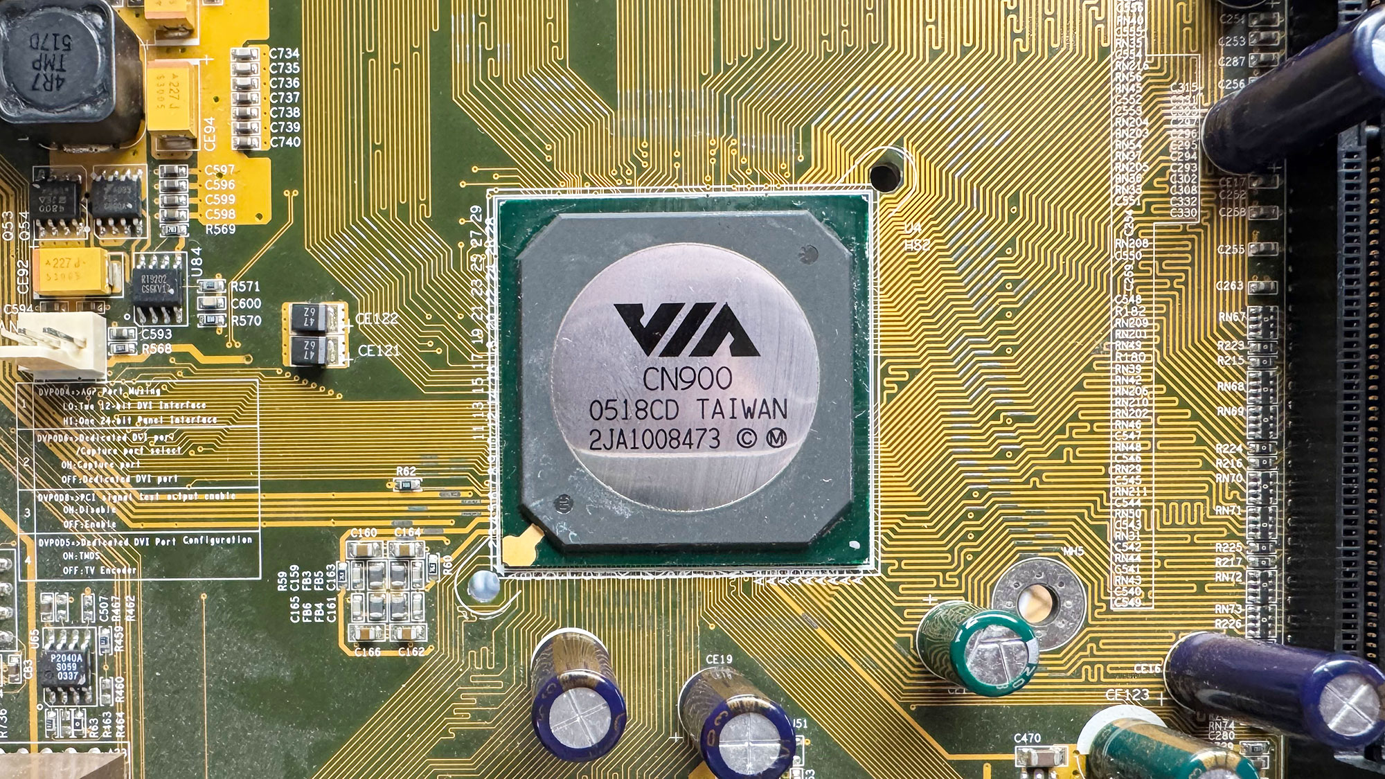
The Esther core connects to the chipset through VIA’s proprietary V4 front-side bus, with effective bus rates commonly specified at 400, 533, or 800 MT/s depending on the processor model. Although the package was mechanically related to Intel’s Pentium M Socket 479 ecosystem, the V4 bus did not use Intel’s AGTL+ quad-pumped (QDR) electrical interface. It was a VIA-specific signaling implementation intended to provide similar platform integration without being electrically compatible with Intel’s bus to avoid legal issues. On the VT5910A, the CPU is linked to the unreleased (and even unannounced) CN900 chipset:
Unreleased VIA CN900 Northbridge
While the CN400, CN700, and CN800 are well documented, I have not found any public reference to a CN900 chipset. This Northbridge shares the same PCI ID and BIOS reference ID as the P4M800 Pro, which was announced in September 2005. The P4M800 Pro was originally designed for the Pentium 4 bus, then later adapted for VIA’s C7 bus and eventually released as the CN700. Internally, both the P4M800 Pro and CN700 are known as the VT3344 Northbridge. The later CN800 dropped AGP in favor of PCI Express, so it is clearly a newer chip. My best guess is that CN900 was a preliminary development name that was later changed to CN700.
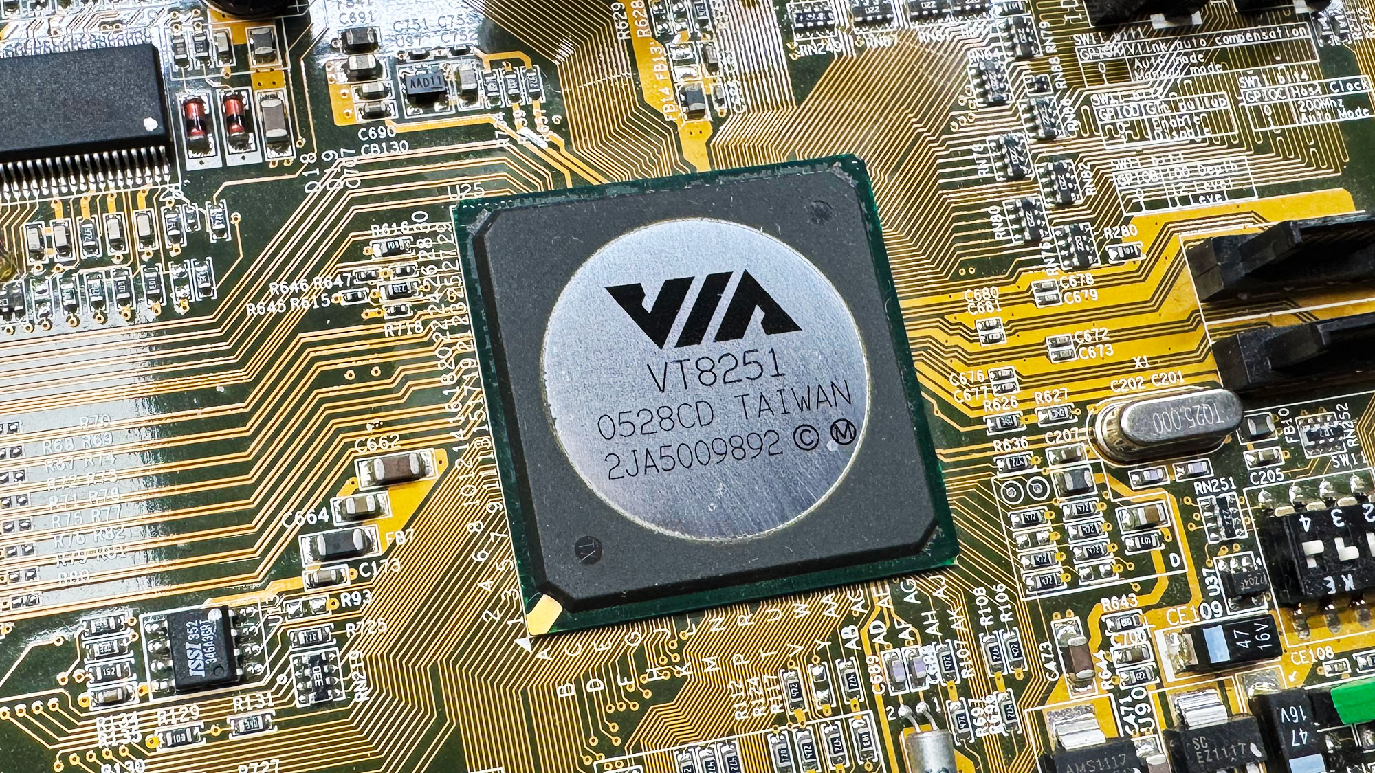
The CN900 includes an integrated S3 UniChrome Pro IGP, internally connected through AGP 8x. It also supports an external AGP 8x slot. Both DDR and DDR2 memory are supported. The VT5910A development board has two DDR2 slots, supporting up to DDR2-667, and one DDR slot, supporting up to DDR-400. This is rather uncommon, but it makes sense for a development board intended to test both memory generations. The PLL and DIP switches show a supported FSB range from 100 MHz all the way up to 400 MHz, which is quite extreme. Another very interesting aspect of the VT5910A is the Southbridge it uses: the VT8251.
Early VT8251 SouthBridge
Back in 2005, VIA, like many other third-party chipset suppliers, was still tied to the aging VT8237 Southbridge. It lacked several modern technologies introduced by Intel in 2003 and 2004, including HD Audio, SATA-II, and, most importantly, PCI Express. The VT8251 Southbridge present on this board was still at an early stage of development. It is quite rare to find a board combining PCI, AMR, AGP, and PCI Express slots.
The BIOS bootup string is “(CC591015) EVALUATION ROM – NOT FOR SALE” and the BIOS ID string is “09/13/2005-P4M800Pro-823-6A7L6009C-00”. Menus have various debugging settings, as expected.
The 6A7L6009C identifier was also used on some commercial boards featuring the P4M800 Pro, such as the MSI MS-7104 and the Top Star TM-P5M8Pro. However, both of those boards use the older VT8237 Southbridge. The only known commercial board pairing the P4M800 Pro with the VT8251 Southbridge appears to be the ASUS P5VDC-MX.
The VT5910A BIOS is available here for download: VT5910A_BIOS
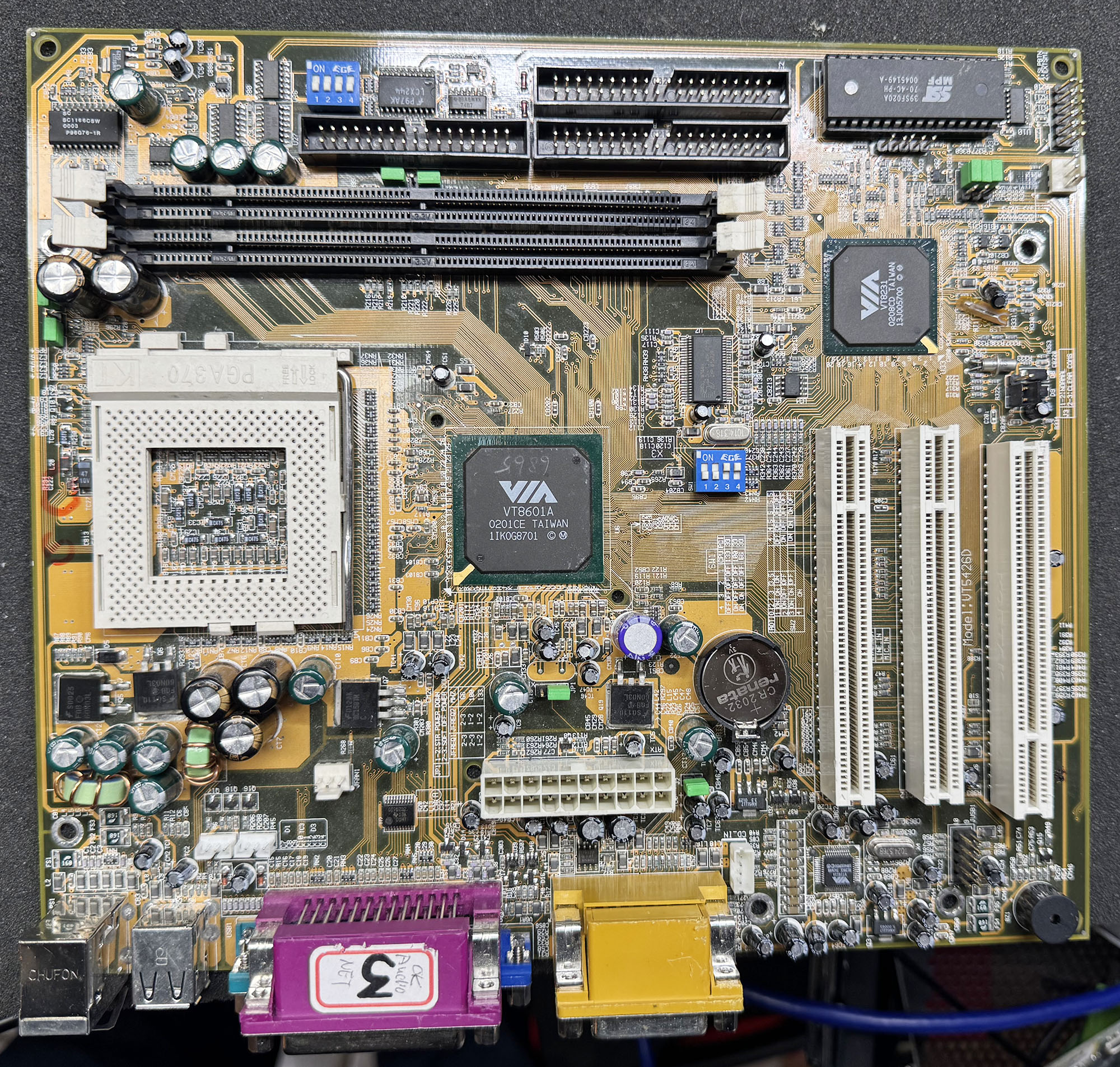
At first sight, the VT5426D board is very similar to the previously analyzed VT5292A. Both are based on the Apollo PLE133 chipset with a VT8601A Northbridge, and large areas of the PCB, especially around the CPU and VRMs, are almost identical. On the newer board, we can also notice the lack of a third SDRAM slot, the missing ISA slot, and the last PCI slot replaced with an ACR slot (physically a reversed PCI slot slightly shifted toward the rear).
VIA VT5426D Development Board
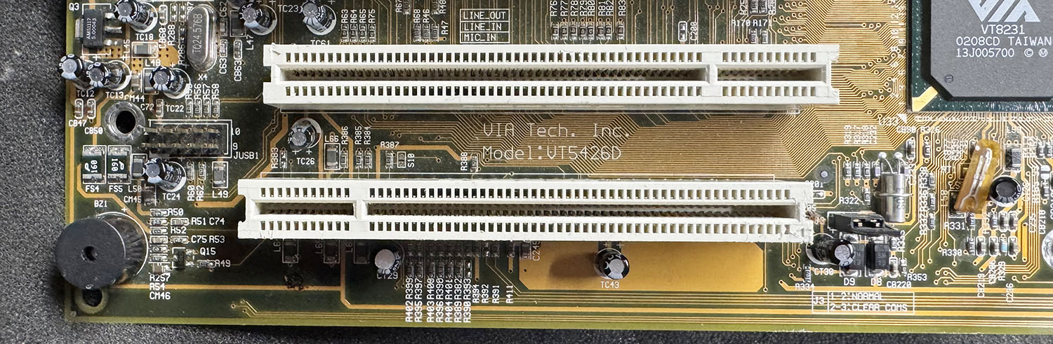
The ACR (Advanced Communication Riser) was a short-lived PC expansion-card standard introduced around 2000 as a successor or alternative to AMR and CNR. It was developed by the ACR Special Interest Group, founded by companies including 3Com, AMD, ALi, Conexant, Lucent, Motorola and VIA. It provided a low-cost riser slot for communication and multimedia functions such as software modems, LAN, broadband, wireless networking, and AC’97 audio, while relying on the motherboard chipset for much of the logic. In practice, ACR was mainly used on a limited number of early-2000s motherboards and was quickly phased-out by more integrated onboard functions.
ACR Slot
But the main difference is obviously the Southbridge, as the VT5426D is based on the newer VIA VT8231, while the previous VT5292A used the older 686B. The difference between the two is small: basically, the VT8231 is a 686B with an integrated 10/100 Ethernet MAC controller. That’s quite strange, because the VT5426D does not have an onboard PHY to make it usable. My first guess was that this board may have been used specifically to debug an ACR card, which could carry a simple PHY and provide a cheap network interface. But the timeline does not quite match: this VT5426D is a late-2001 board using an early-2002 chipset, while the first ACR 1.0 specification was announced in February 2000, almost two years earlier.
So why the hell did VIA produce a new development motherboard lacking the required PHY and RJ45 connector to test the only new feature of its new Southbridge? Let’s try to boot this board and continue the investigation. Fortunately, as with the previous one, it has very little damage and no bad capacitors (I promise this won’t be the case with all the other boards…). The board booted fine on the first try.
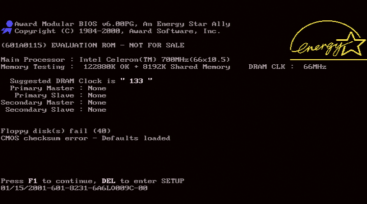
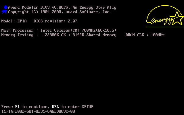
The Award BIOS string identifier for the VT5426D is “01/15/2001-601-8231-6A6LO009C-00”.
The startup string is “(601A0115) EVALUATION ROM – NOT FOR SALE”.
That’s quite interesting. The BIOS is dated January 2001, while the board appears to have been assembled more than a year later: the chipset manufacturing date is late February 2002. This is very unusual, as BIOSes from this era were usually updated quite frequently to support the latest CPUs. The only reason to use such an old BIOS would be for a fixed hardware configuration over a long-term period, for example with the same CPU. Indeed, all mentions of settings dedicated to supporting various CPUs, which were present on the VT5292A, have been removed from the PCB silkscreen.
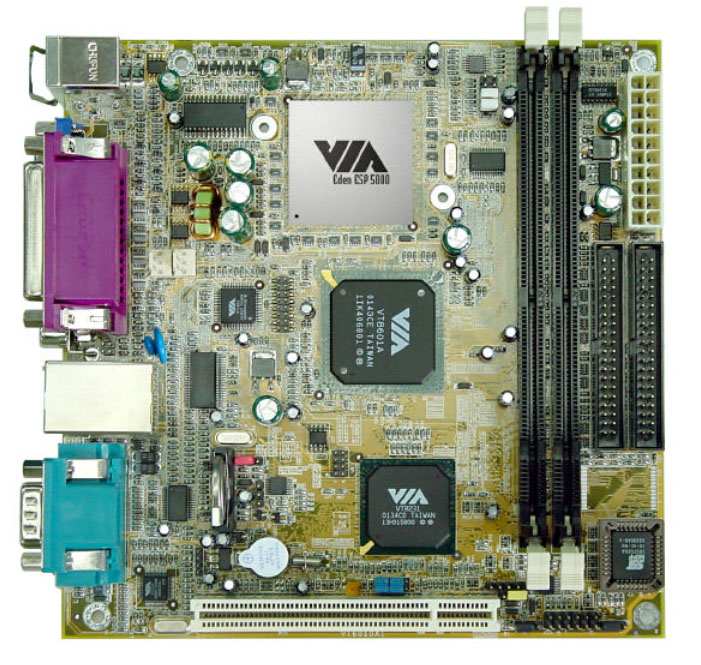
But the most obvious hint about the true nature of this board is the BIOS identifier: “6A6LO009C”. This exact ID was used by VIA for the very first EPIA board, announced in April 2002. EPIA, for Embedded Platform Innovative Architecture, was VIA’s compact motherboard family for low-power embedded and small-form-factor x86 systems, introduced in the early 2000s as part of the company’s push toward highly integrated “platform” designs. Built around VIA C3/Eden processors and VIA chipsets, EPIA boards combined the CPU, graphics, audio, networking, storage, and legacy I/O on very small Mini-ITX boards (a very compact 17 × 17 cm form factor introduced at the same time and still used today).
It looks like VIA gradually shrank a PLE133 reference board, from MicroATX to the initially proposed “ITX” form factor, and finally to the much more ambitious Mini-ITX form factor, with the following timeline:
January 2001 : VT5426D Development MicroATX form factor (24.4 x 24.4 cm), Socket 370.
March 2001 : VT6009 Development board in the first proposed ITX form factor (21.5 x 19.1 cm), Socket 370. Note the ACR port. Following the success of this board at CeBit 2002, VIA probably decided to shrink the form factor even more.
November 2001 : VT6010 Reference board for the final Mini-ITX form factor (17 x 17 cm), Soldered VIA Eden ESP (low voltage VIA C3)
April 2002 : First commercial Mini-ITX boards under the EPIA line. Soldered C3 (EPIA 800, fan) or Eden (ESP 5000, fangless) CPU.
All these boards are based on the Apollo PLE133 chipset with the VT8231 Southbridge and use the same overall schematics, with the same PLL, audio codec, BIOS flash chip, and a similar architecture.
These boards were so similar, and the VT5426D shares so much with the final EPIA board, including its BIOS identifier, that I had a crazy idea: what would happen if I flashed the commercial EPIA BIOS onto the VT5426D? Had VIA removed support for Intel CPUs from the final EPIA BIOS, considering that commercial EPIA boards were only available with soldered VIA CPUs? Or had they kept the code inherited from older development boards, which supported any Socket 370 CPU? Let’s try it.
EPIA 800 Commercial BIOS booting on VT5426D board
Bingo! The board booted immediately with the EPIA logo and was fully functional, except for the missing network part. It’s quite odd to see a VIA EPIA BIOS running with an Intel Celeron Coppermine CPU. So, in the end, the best guess is that the VT5426D was the missing link that ultimately led to the first EPIA Mini-ITX board.
You can download the original VT5426D BIOS, dated 01/15/2001, here: VT5426D_BIOS
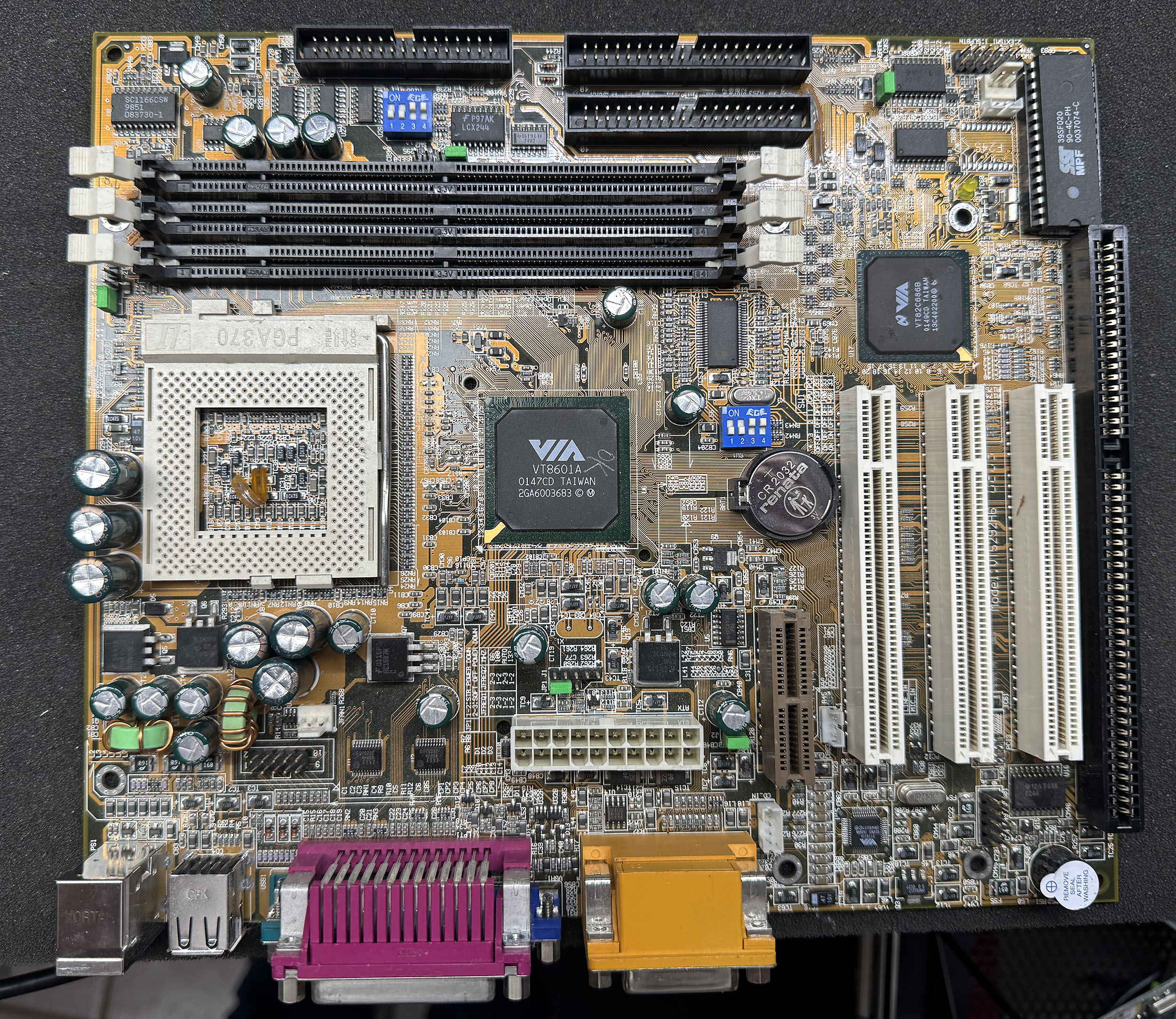
Let’s continue the series with another one of the least damaged boards: the VT5292A, built around the Apollo PLE133 chipset, with a VT8601A Northbridge and a VIA VT82C686B Southbridge. This chipset was the direct successor to the MVP4 in VIA’s “integrated” chipset line, with built-in graphics. This time, we have Socket 370 and three SDRAM slots supporting PC66, PC100, and PC133 modules, up to 1.5 GB. The IGP is still from Trident, but upgraded to their Blade3D line. The 686B Southbridge supports USB 1.1 via UHCI, IDE ATA-33/66/100, AC’97 audio, PCI 2.2, and an integrated Super I/O controller. It also includes an integrated PCI-to-ISA bridge.
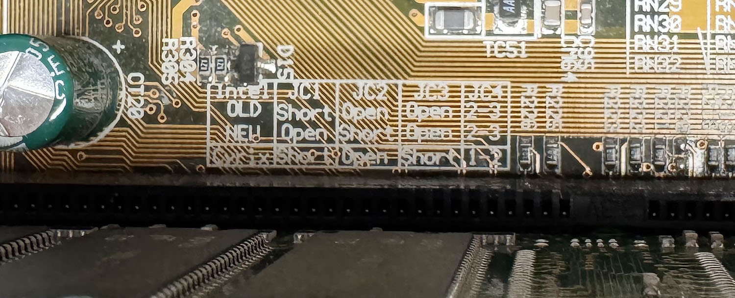
The board arrived quite clean, without major damage and with capacitors that were visually in good condition. Many jumpers were unfortunately undocumented, and it took quite a long time to figure out how to boot a Celeron or Pentium III Coppermine. The VT5292A supports FSB settings from 66 to 133 MHz and requires jumper configuration to select between three CPU types: “Cyrix”, “Old Intel”, and “New Intel”. The latter is obviously for Coppermine CPUs, while the “Cyrix” setting was targeted at VIA C3s, formerly Cyrix III.
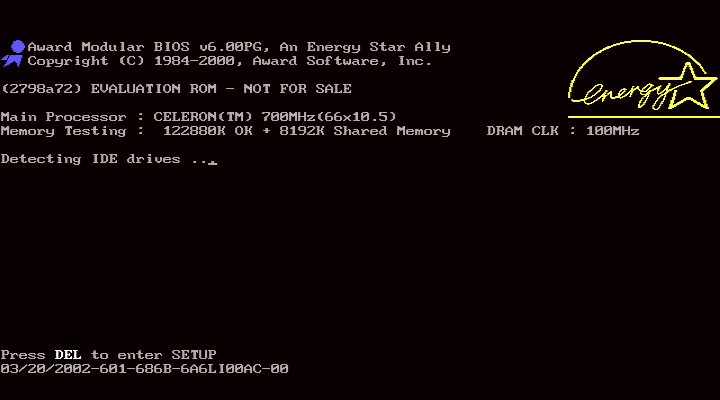
The Award BIOS string identifier for the VT5292A is “03/20/2002-601-686B-6A6LI00AC-00”. The startup string is “(2798a72) EVALUATION ROM – NOT FOR SALE”. The mainboard identifier, “6A6LI00AC”, is the same as on the Soyo SY-7VEM, which looks almost identical except for the number of DIMM slots: the Soyo only has two slots, while the VT5292A has three. The location of some headers is also slightly different, but it looks like Soyo simply rebranded the Apollo PLE133 reference board as its own model, which was quite common back then.
The BIOS has a lot of debugging options, especially related to the IDE controller. This may be related to the onboard VT82C686B, the first VIA Southbridge to support ATA-100; the previous 686A was limited to ATA-66. The rest of the BIOS is quite standard, with a decent temperature, voltage, and fan-speed monitoring page. The CPU temperature sensor is still external on this board, with a thermocouple positioned just behind the CPU. This board may look like one of the least interesting ones at first, but it will soon become more important, as it represents an evolutionary step toward the next board we will check: the VT5426D.
The VT5292A motherboard BIOS is available here: VT5292A_BIOS
Some years ago, one of the last remaining VIA R&D facilities closed its doors, and I was lucky enough to save a bunch of motherboards from the salvage bin. Most of them were rare reference boards and development boards from the late ’90s and early 2000s, with sockets ranging from Socket 7 to Socket A/423, or with embedded VIA CPUs.Unfortunately, all these boards had already been prepared for e-waste, with some components, such as heatsinks, brutally ripped off before the boards were roughly tossed into a bin, causing various damage to the components and PCBs.In this series, I will try to get them working one by one, repairing the damage they suffered and documenting my findings.
Let’s start with one of the less damaged boards. This VIA VT5182E MicroATX reference motherboard is built around the Apollo MVP4 chipset, with a VT8501 Northbridge and a VIA VT82C686A Southbridge. It’s a “Super” Socket 7 board, supporting later Socket 7 CPUs, including 100 MHz FSB chips such as the Cyrix MII, the AMD K6-2 and K6-III, the IDT WinChip 2, and others. The VT8501 can also work with FPM/EDO DIMMs, but this board only supports modern PC66/PC100 SDRAM. There is no AGP slot here because the VT8501 already integrates a Trident CyberBlade i7 IGP, or integrated graphics processor, on the internal AGP bus, using shared memory. The 686A Southbridge supports USB 1.1 via UHCI, IDE ATA-33/66, AC’97 audio, PCI 2.2, and an integrated Super I/O controller.
The VT5182E reference board had little damage, withonly a couple of scratches on the PCB and no cut traces. There were no bulging capacitors either. The board has quite a lot of jumpers, with FSB selection from 66 to 124 MHz, multiplier settings from 1.5x to 5.5x, and Vcore from 2.0 V to 3.5 V. A UMC UM616464AF-5 chip adds 512 KB of L2 cache. The only oddity is a very (very) bad rework near the audio jack, with various THT components, including resistors and capacitors, soldered Manhattan-style and brutally glued together into one big messy blob. It was probably a quick-and-dirty fix by an engineer in the lab.
The board was able to boot with a PCI graphics card, but the onboard VGA port only displays a corrupted image. Resoldering the VGA port solved the issue. The Award BIOS string identifier for the VT5182E is “04/13/1999-VP4-686-2A5LE00DC-00”. The startup string is “(R34-5182) EVALUATION ROM – NOT FOR SALE”. The BIOS is fully featured, as expected for a reference board, but lacks the shiny jumper-less configuration feature.
Let’s now guess what this board was used for. The Apollo MVP4 chipset was announced in August 1998, with availability in Q4’98. This VT5182E board has a BIOS dated April 1999. According to their engraved date codes, almost all components of the boards (Northbridge, cache chip, PLLs, EEPROM, MOSFETs, etc.) were manufactured between Q3’98 and Q1’99. The real oddity is the 686A Southbridge, dated WW23’2000, more than a year later. It’s almost certain that the Southbridge on this board was replaced at some point with a much newer revision. The timeline coincides with the development of the 686B Southbridge, which added ATA-100 and fixed some bugs, while adding a couple of new ones.
The VT5182E motherboard BIOS is available here: VT5182E_BIOS
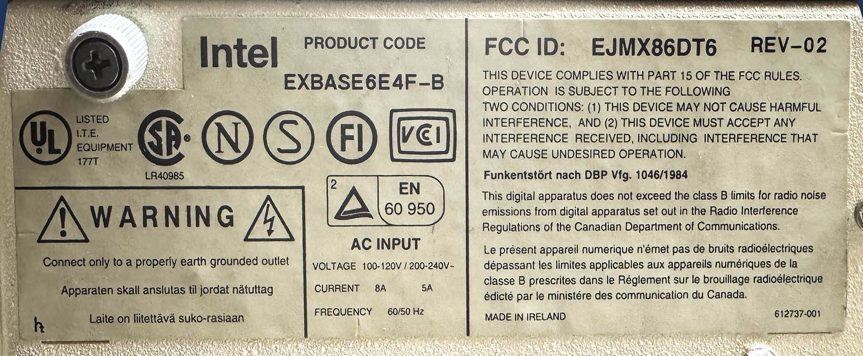
I’ve just finished restoring one of the few computers Intel produced in the early 1990s, and I’d like to share a few pictures of this wonderful platform. It has all the ingredients to catch the eye of retro enthusiasts: a full EISA motherboard, a design that served as the reference platform for the infamous 50 MHz 486DX and the original Pentium 60 MHz, a unique chipset found nowhere else, modular CPU boards, and more. Launched in 1992 and discontinued in 1995, the Intel Xpress product line sat somewhere between the personal computer and the workstation. These were not ordinary home PCs, but modular, expandable machines built for professional and networked business use (and also built like tanks). Three versions were produced: the Xpress Desktop, the Deskside/LX (tower/server), and the Deskside/MX (tower/server with SCSI). The latter models were also rebranded by HP as part of its early NetServer line. A few months ago, I bought an Xpress Desktop from Germany in very poor condition, and it clearly deserved some love.
The motherboard and chipset
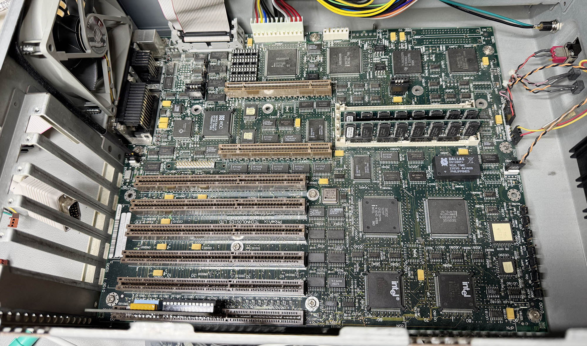
Let’s start with the motherboard. The entire Intel Xpress line was built around two main boards: the 6-slotused in the Desktop, and the larger 8-slot XBASE6TE8F for the Deskside server chassis, available in SCSI and non-SCSI versions. Here is the board that came with my Xpress system:
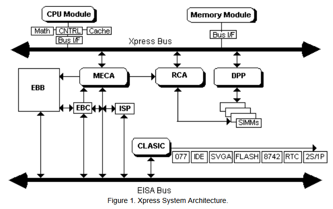
Fortunately, a complete parts and revision log for the Xpress series has survived, which made it possible to identify this board in more detail. The PBA 519610-004 sticker indicates that it is the 10th revision out of a total of 14, manufactured in July 1993. As expected, the motherboard is equipped with 6 EISA slots. The board is built around two distinct chipsets that divide the work between the system core and the expansion bus: Intel’s own Xpress chipset, which handles the processor, memory, cache coherency, and onboard I/O, and a separate EISA chipset, which manages communication with the EISA/ISA expansion bus.
On the Xpress side, the MECA (Memory to EISA ASIC – 82356CS) links main memory to the EISA bus, arbitrates access between the CPU and bus masters, manages memory decoding, and supports cache snooping as well as parity or ECC memory; the RCA (RAS/CAS Control ASIC – 82356DS) controls DRAM timing and addressing, generating the RAS/CAS signals and handling the multiplexed addresses for the 64-bit memory subsystem; two DPP (Data Path Parity – 82353DS) chips provide parity generation and checking for the wide DRAM data path; and the CLASIC (Common Local ASIC – 82351DS) takes care of local peripherals and system I/O, including the video controller, flash memory, EISA ID logic, and standard ports such as floppy, IDE, serial, parallel, and mouse.
Alongside it, the EISA chipset handles the expansion side of the machine: the EBC (EISA Bus Controller – 82358DT) translates CPU commands into EISA and ISA bus operations and controls bus cycles, DMA, bus-master access, and data steering; the ISP (Integrated System Peripheral – 82357) integrates core system functions such as DMA channels, timers, interrupt controllers, refresh logic, and EISA arbitration; and the EBB (EISA Bus Buffer – 82352) provides the physical buffering, latching, and parity support needed for reliable address and data transfers on the EISA bus.
The two slots on top of the EISA physically look like PCI slots, but they are dedicated to CPU and RAM daughter boards. Of course, the battery inside the original Dallas DS1287 RTC/CMOS chip was fully depleted and had to be replaced with a modern compatible DS12887+ chip. Luckily, the original Dallas chip was socketed and not soldered on the board. I added two 16 MB DIMM memory stick with ECC parity (x36 bus) as the board doesn’t accept standard 32-bit DIMMs.
CPU Boards
Up to 12 CPU boards were available for the Xpress motherboards, covering nearly the entire range of 486 and early Pentium processors: 486SX/25, SX/33, DX/33, DX/50, DX2/50, DX2/66, DX4/100, as well as the Pentium 60, 66, 90, and 100. There was even a rare dual-processor board featuring two Pentium 66 MHz CPUs in SMP, compatible only with later revisions of the 8-slot EISA motherboard. I was lucky enough to find three different boards, including the most iconic.
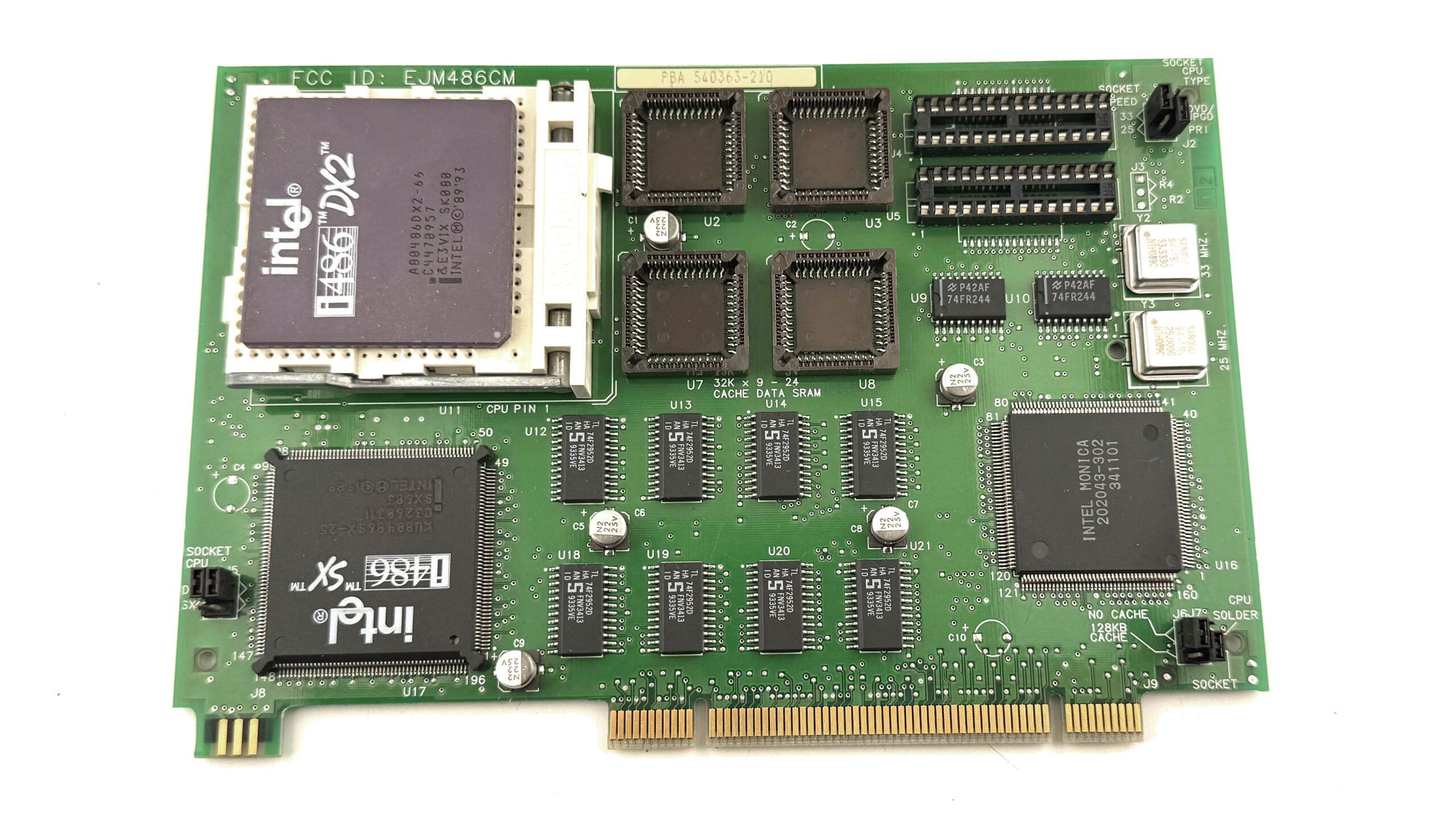
EJM486CM
This EJM486CM/BXCPU486SX25 (PBA 540363-210) is the latest revision of the most affordable CPU board in the range. It comes with a low-cost 486SX/25 processor soldered directly to the board, but also includes an empty Socket 3 ZIF socket for a CPU upgrade. It can accept an OverDrive processor or virtually any 5-volt 486 up to a DX2/66. Intel fitted the board with two quartz oscillators, 25 MHz and 33 MHz, allowing a single jumper to select either one. A second jumper is used to choose between the onboard CPU and the one installed in the socket. No L2 cache is fitted as standard, but 128 KB can be added later by the user with 4x 32 KB PLL chips and 2x DIP Tag RAMs.
BXCPUPENT66
I also managed to find a very nice BXCPUPENT66 (614023-006) board, fitted with the legendary 66 MHz Pentium. The Xpress platform also served as Intel’s reference system for debugging the original Pentium before its official release. A number of pre-production CPU boards based on the Pentium 60 MHz are documented from the period leading up to the 1993 launch of Intel’s first Pentium processor. The purpose of the large PCB interposer placed between the CPU and the CPU board is especially interesting: it is a massive DC-to-DC voltage converter used to raise the motherboard’s +5V supply to +5.4V. This was a rather crude last-minute fix, added because the Pentium 66 MHz, originally meant to run at 5V, proved unstable at that voltage. It made the CPU’s overheating problem even worse, but at least it allowed the system to operate reliably.
This high-end CPU board is also equipped with an expensive Intel 82496 cache controller and eight Intel 82491 32 KB SRAM chips, for a total of 256 KB of write-back L2 cache running at full speed with no wait states. That was truly state of the art in 1994! The CPU on my board is also a C1 stepping part, which means it is affected by the infamous FDIV bug.
BXCPU48650
But the board that will definitely stay in this Xpress Desktop is the BXCPU48650, because nothing suits the machine better than a proper 486 DX 50 MHz (not to be confused with the slower DX2-50). Among 486 processors, the DX-50 has always had a special reputation. Unlike the far more common DX-33, DX2-66, or DX4-100, which all relied on a 33 MHz external bus and reached higher internal speeds through clock multiplication, the 486DX-50 ran both the CPU and the front-side bus at a full 50 MHz. That made it one of the most aggressive 486 designs Intel ever put into production. Intel announced the 50 MHz 486DX in 1991, but it never became a mainstream part, in large part because pushing an entire 486 platform to a true 50 MHz bus placed heavy demands on the motherboard, chipset, cache, and expansion subsystem (especially ISA).
As a result, only a few high-end motherboards offered stable DX-50 support, and the processor was soon overshadowed by the more practical DX2-66, which delivered better overall performance while keeping the external bus at a far easier 33 MHz. The DX-50 was therefore a short-lived dead end in commercial terms, but that’s precisely the reason why it became legendary: it represents the 486 generation pushed right to the edge, before clock-doubling became the cleaner solution. For a machine like the Intel Xpress, with its unusual architecture and reference-platform pedigree, the BXCPU48650 feels like the most historically fitting choice.
Now it’s time to fit the beast with some nice cards!
EISA cards
The EISA bus (Extended Industry Standard Architecture) was one of the early 90s’ attempts to improve the old ISA standard used in IBM-compatible PCs. It was mainly designed for high-end desktops, workstations, and servers, and offered a wider 32-bit data path, bus mastering, and more advanced setup features. One of its biggest advantages was that it stayed fully compatible with older ISA cards, so an EISA machine could still use existing expansion hardware. This made it a good transitional technology rather than a complete break from the past. Even so, EISA did not last very long. It was mostly used in expensive systems, and during the 486 era it had to compete with VESA Local Bus (VLB), which was especially attractive for graphics and storage. In the end, both were replaced by PCI.
Finding EISA cards today is quite difficult, but I had saved a few over the years for a good project like this one.
Compaq QVision 1024/E VGA
The first one is a Compaq QVision 1024/E VGA card for the EISA bus. It has 1 MB of video RAM, a Brooktree Bt484 RAMDAC, and a rare Motorola SC02SH007DK04 graphics chip. As far as I know, no datasheet or detailed documentation for that chip has survived, so its exact features are still unknown. What benchmarks do show, however, is that the QVision 1024/E is much faster than its ISA version (QVision 1024/I). It is also faster than a good ISA card based on the Tseng Labs ET4000, and under DOS it reaches about 80% of the performance of a Matrox Millennium (PCI), which is very impressive for an EISA graphics card.
3Com 3C597-TX EISA Fast-Ethernet (100 Mb/s)
Next one is a 3Com 3C597-TX network card. It is an EISA Fast Ethernet adapter with a standard RJ45 port, supporting both 10Base-T and 100Base-TX networking over twisted-pair cable. That already makes it a rather unusual card for a machine like this, because true 100 Mbit/s Ethernet was still a high-end feature at the time and was mostly found in serious workstations and servers rather than ordinary desktop PCs. The 3C597-TX is a 32-bit EISA card, and 3Com marketed it as part of its Fast EtherLink family, with bus-mastering support and an optional boot ROM for network boot environments. In a system like the Intel Xpress, it feels completely at home: period-correct, very capable, and a good reminder that this platform was designed for professional networking as much as raw CPU performance.
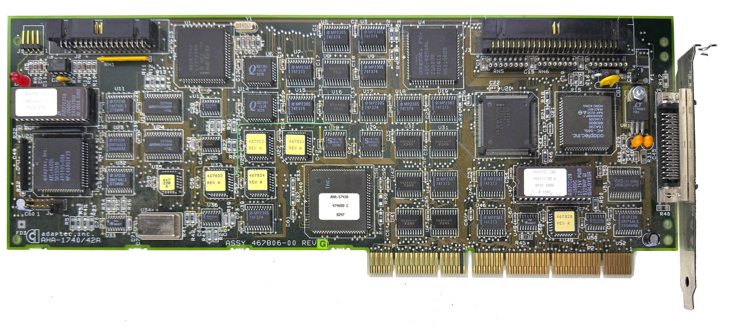
Adaptec AHA-1742A SCSI EISA
And then, the behemoth of EISA cards, the Adaptec AHA-1742A. This is a full-length, full-height EISA-to-Fast SCSI host adapter, built for serious storage hardware rather than ordinary desktop use. The card is a 32-bit bus-mastering controller, designed to link the EISA bus to single-ended Fast SCSI, and it supports up to seven SCSI devices on the bus. It also includes both an internal 50-pin SCSI connector and an external HD50 port, plus a floppy controller header on the card itself. Adaptec marketed the 1742A as a high-performance solution, and period documentation quotes EISA burst transfer rates up to 33 MB/s, which gives a good idea of the kind of system this card was meant for: servers, workstations, and other heavy-duty machines where storage performance really mattered.
In a machine like the Intel Xpress, the AHA-1742A feels absolutely right. It is oversized, overbuilt, and exactly the sort of premium expansion card you would expect to find in a high-end EISA system from the early 1990s. To make things even better, I connected it to a Plextor 12/20x CD-ROM drive, which suits the platform perfectly and adds another proper piece of costly high-end hardware to the build.
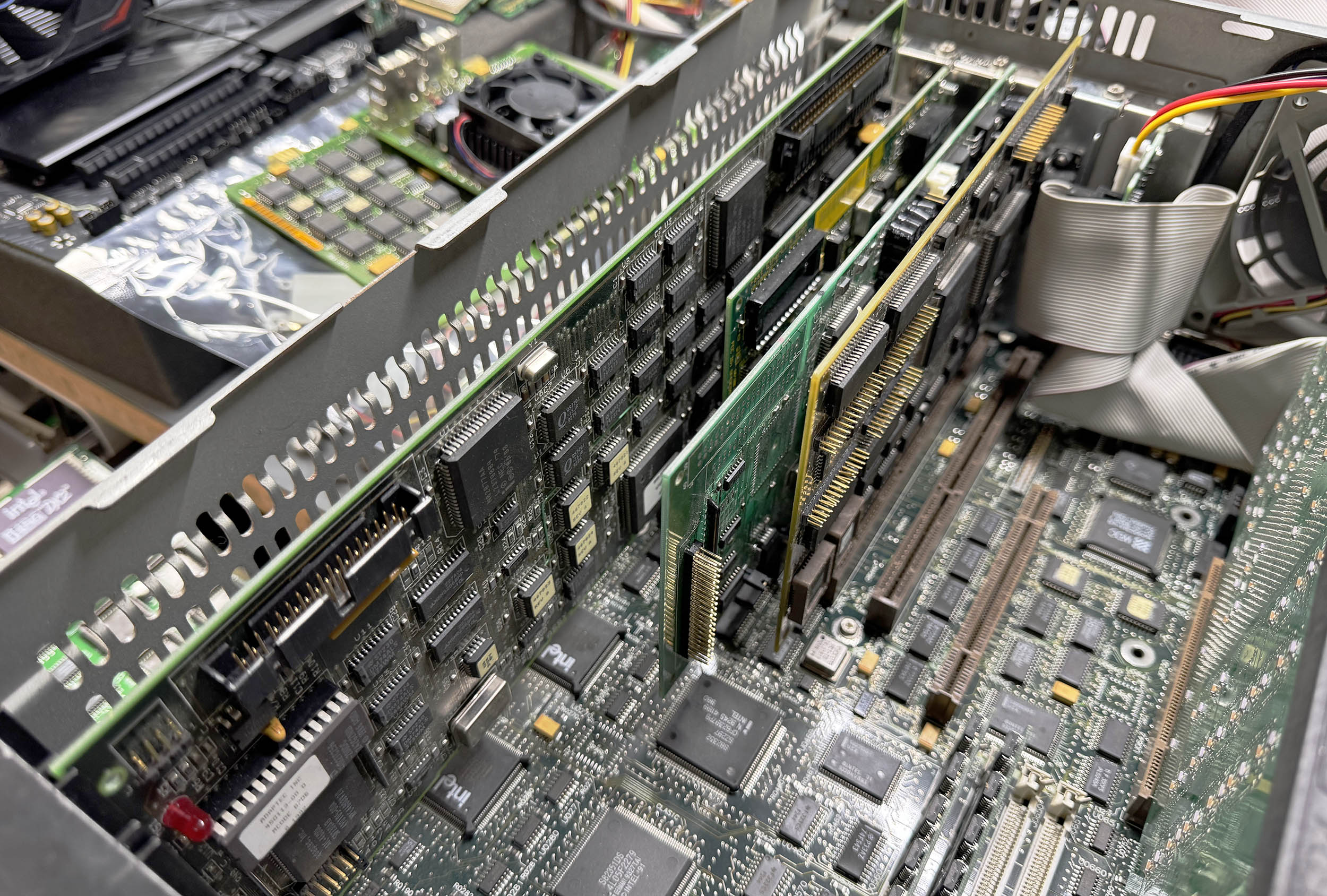
I then replaced the loud 80 mm fan with a Noctua NF-A8, swapped the original AT power supply for an FSP 350W ATX unit connected through an ATX2AT Smart Converter v2 (which happily handled the 10A required on the 5V rail at full load), added a Sound Blaster 16, and finally replaced the noisy, painfully slow 270 MB Quantum ProDrive LPS hard drive with a shiny 4 GB CompactFlash card connected to the motherboard’s IDE interface. To make the CompactFlash card bootable, I added an ISA ROM card loaded with the XT-IDE firmware. After that, I configured all the EISA cards using the proprietary setup utility and configuration files, then installed MS-DOS 6.22 and Windows for Workgroups 3.11. Windows NT 3.51 is next on the list. And yes, it runs DOOM!
A few months ago, I came across what looked like a real gem on eBay US: a studio copy of Intel’s iconic “Bong” sound. Yes! The famous 5-note jingle composed by Walter Werzowa in 1994 and used by Intel since the Pentium II era (starting in 1996).
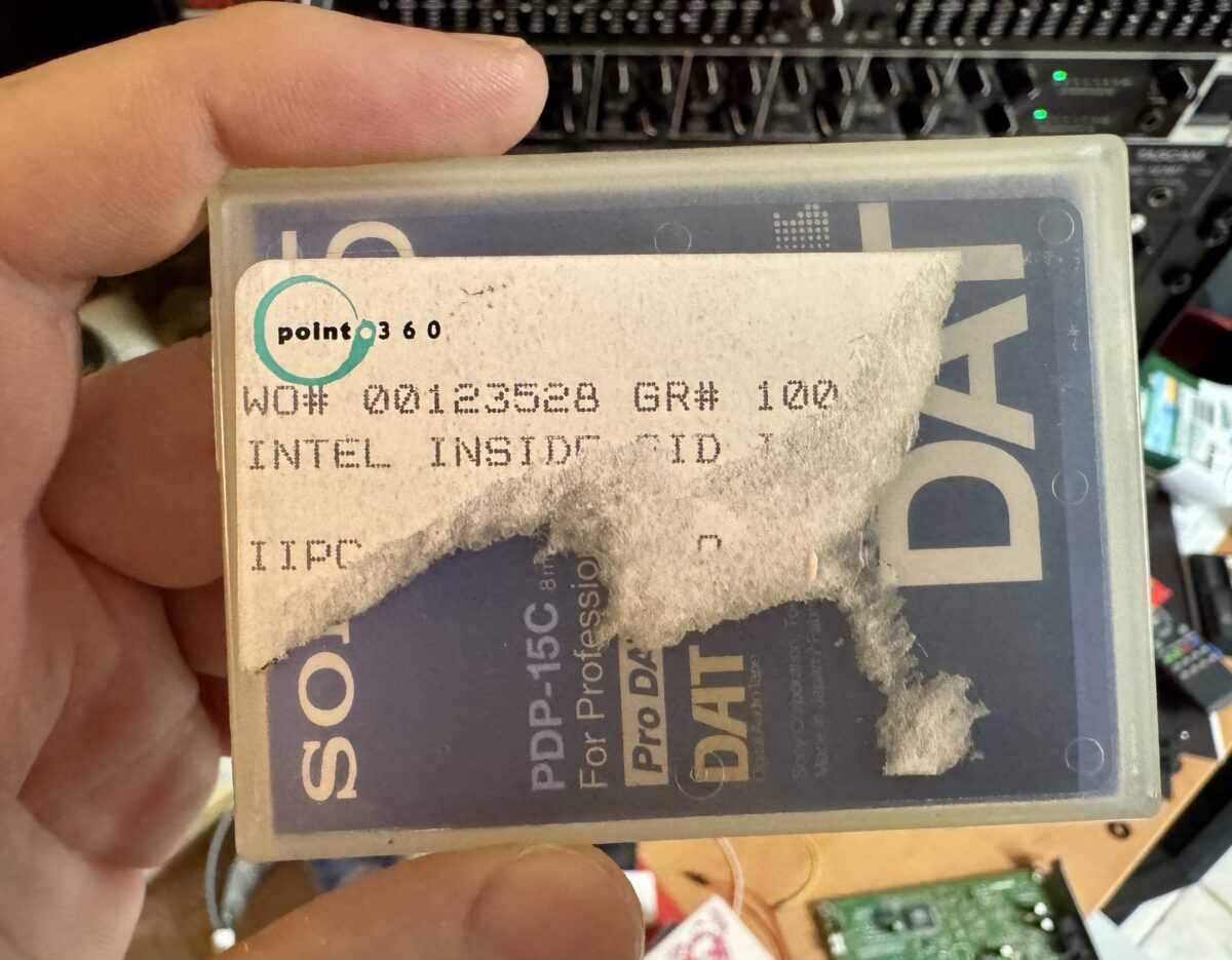
According to the seller, the tape is a digital DAT (Digital Audio Tape) master from the post-production company Point.360 (still in business today), which worked with Intel in the 90s. The label on the tape had been torn, but some details are still readable: an Intel internal identification number (IIPCxxxx), along with other IDs (WO# 00123528 / GR #100).
I promptly bought it and then began the hunt for a decent DAT player locally. That stuff is still pricey! In the end, I found a refurbished Sony DTC-790 at a good price so I could test the tape. Here’s the result:
After about 20 seconds of the standard calibration tone, a female voice says: “This is for Intel Corporation. ID number IIPC5100. Audio signature ID for the Intel Inside Pentium III Processor for Worldwide use.” followed by the famous bong! What a nice treasure!
This isn’t the very first version used for the Pentium II, but the second revision used from 1999 to 2006 for the Pentium III and Pentium 4. Personally, I find this version the most iconic (the earlier one sounds much less dynamic to my ear). You can listen to all the revisions of the “bong” (there are dozens) on this website.
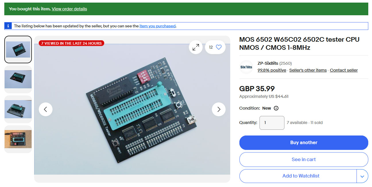
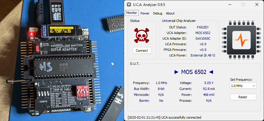
During the beta-testing phase of the Universal Chip Analyzer (UCA), some testers noticed that certain CPUs failed on the UCA while appearing to work on more basic testing devices. To determine whether this discrepancy was due to a flaw in the UCA, I purchased a couple of these simpler testers for comparison. Out of five 6502 CPUs that the UCA had flagged as defective, two passed without any issues on the basic testers. To verify their actual condition, I tested them in a real Apple IIe. Both failed to boot the system, prompting me to analyze their behavior further using a logic analyzer.
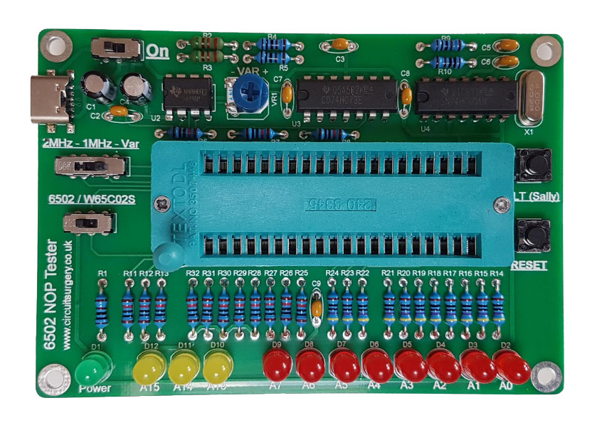
To understand why this happens, it’s important to look at how common CPU testers—readily available on eBay and other marketplaces—operate. The simplest type, known as a “NOP Tester,” provides a basic clock signal, often generated by a simple oscillator such as a NE555 timer. It permanently feeds a NOP (No Operation) instruction to the CPU’s data bus, instructing it to do nothing except cycle through all addresses indefinitely. In a 6502, the NOP instruction is represented by 0xEA (in binary: 1110 1010), which is hardwired onto the data bus. If the address bus increments smoothly and continuously, indicated by LEDs displaying changing values, the CPU is considered functional.
6502 NOP Tester from circuitsurgery.com
More advanced testers, like the ones I purchased, incorporate an EPROM containing pre-programmed test code. These devices use 74HCT245 bus transceivers to drive LEDs that display the 16-bit address bus (A0-A15) and a 74HCT574 flip-flop to control an 8-LED moving dot pattern on the data bus. The ROM feeds instructions to the CPU, allowing for slightly more complex testing than a simple NOP Tester.
6502 ROM Tester from eBay
However, despite being more sophisticated, EPROM-based testers still fall short of replicating a real computer environment. Unlike a basic tester, an actual computer relies on RAM, external peripherals, and extensive arbitration logic to manage operations. This is why CPUs have so many additional pins beyond just data and address lines. For instance, the 6502 includes bus arbitration signals like READY, IRQ, NMI, READ/WRITE, SYNC, SO, and derived clock signals Ø1 and Ø2. Most cheap testers either ignore or fail to adequately evaluate these critical signals. In contrast, the UCA is designed to comprehensively test every CPU pin, accurately simulating ROM, RAM, stack operations, interrupts, and other essential functions found in real-world systems.
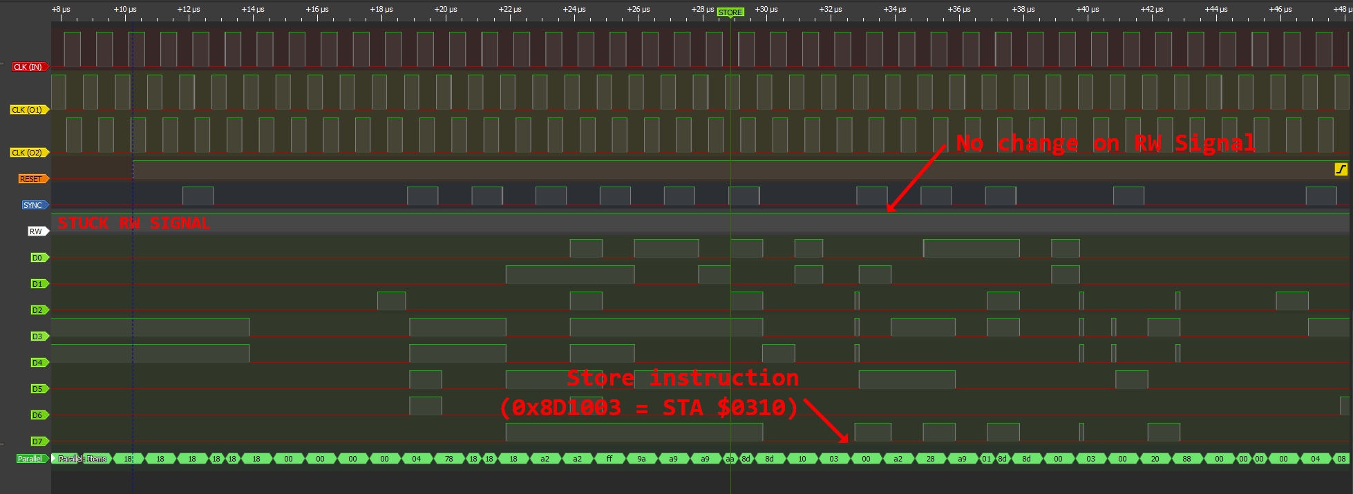
The logic analyzer helped pinpoint the exact issue: the R/W (Read/Write) pin on the two defective 6502s was stuck high (logic 1). This rendered them unusable in real computers and on the UCA, yet they still appeared functional on the basic testers.
Defective 6502 on Logic Analyzer (Click to Zoom)
This highlights the key weakness of cheap CPU testers: they only assess a limited set of CPU functions, sometimes failing to detect faults that would cause real-world failures. The UCA, by contrast, provides a much more thorough evaluation, ensuring CPUs are genuinely functional under real operating conditions rather than just passing a superficial test.
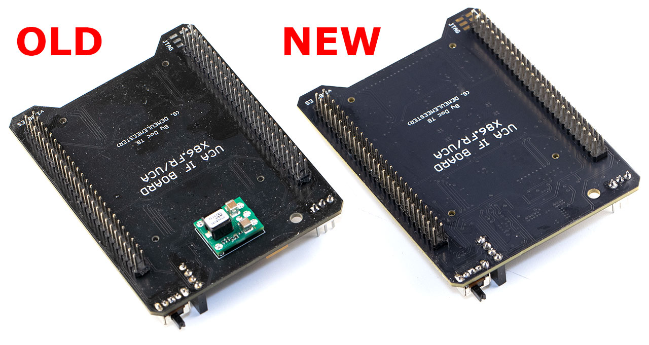
Designing a stable, adjustable and fail-safe power supply for the Universal Chip Analyzer has been one of the most challenging aspects of this project and I was quite reluctant to touch that part of the schematics. For years, the DC-DC power supply stage on the UCA Interface Board relied on Texas Instruments’ PTH08080W module, mounted upside down. While this module is excellent and performs reliably, it has two significant drawbacks.
First, it’s expensive, costing around $8–$9 per unit. Additionally, as a non-standard through-hole component, it complicates assembly and increases costs when using a reflow machine.
More importantly, the PTH08080W module needed to be replaced to implement a highly requested feature from beta testers. Previously, a 9V external power supply was mandatory in addition to the 5V provided by the USB-C to power the UCA Interface Board. That external power supply powered the DC-DC converter, which delivered an adjustable output voltage ranging from 2.8V to 5.5V at up to 2A. However, in some cases (such as testing 5V-only CPUs that consume less than 300mA), the voltage provided by USB-C alone could be strong enough. Beta testers requested an alternative power option to use only USB-C power when it’s possible, and this final revision delivers on that request.
The PTH08080W module has been replaced with a discrete DC-DC converter, complemented by additional circuitry for digital control of the voltage output. An ideal diode controller has also been integrated to manage the USB-C 5V input, ensuring seamless switching and protection in the event of a failure.
The Universal Chip Analyzer now features two automatically selected power modes:
USB-C Only (No External Power)
In this mode, the UCA can test 5V chips that draw less than 300mA. This includes, for example, all DIP40 ICs. Overcurrent and short-circuit protections are still in place, but the UCA will only allow this mode for compatible adapters. This setup is perfect for quick, portable testing in the field using a USB battery pack.
USB-C with 9V External Power
This fully featured mode supports all UCA functionalities, including the ability to test a wide range of components, from early DRAM to late 5×86 chips. Adjustable voltages (e.g., 3.3V, 3.45V) are supported, with high current capability up to 2A. This mode is ideal for advanced bench analysis and testing of more demanding components.
With this final challenge resolved, I’ll be updating the UCA website and opening preorders in two weeks.
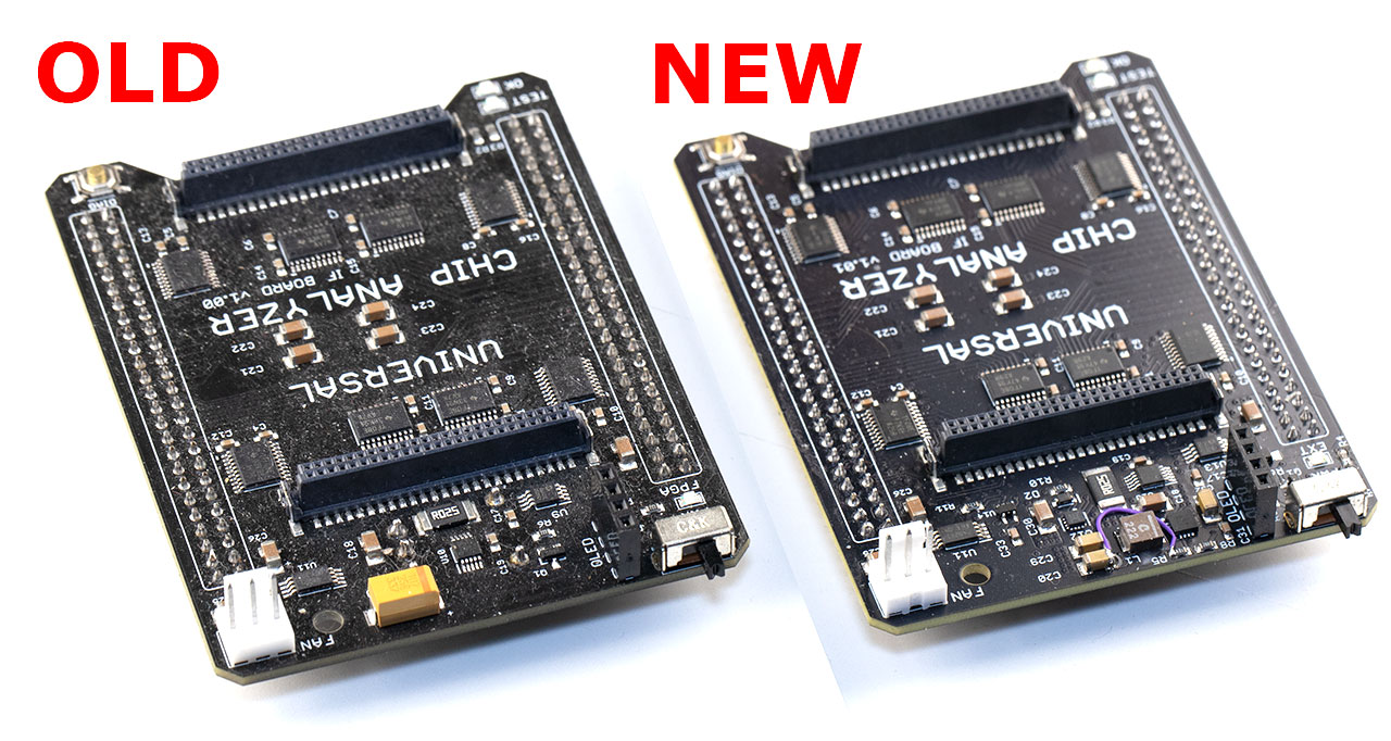
The Universal Chip Analyzer (UCA) beta testing is entering its final phase! Thanks to the valuable feedback from talented professionals and passionate retro enthusiasts, two critical improvements were identified and addressed before the official release. The first improvement concerns the Interface Board, and a detailed update is coming soon. The second key enhancement involves the DIP40 Adapter, which initially required additional top adapters to test common CPUs like the Zilog Z80, Motorola 6800, and MOS 6502.
These extra adapters were necessary because the power and ground pin configurations of these processors differ from those of Intel’s 8085/86/88, for which the original DIP40 adapter was designed. Switching VCC and GND to other pins is technically not very complex, but it’s much more difficult to keep these pins simultaneously usable by high-frequency signals. The transistors required to switch power lines add various parasitic noise to the pins, even when they’re switched off.
I’m happy to announce that the final DIP40 Adapter is now able to test the most common DIP40 CPUs from the 70s and 80s out of the box, without the need for any additional adapters! Here is a comparison of the old DIP40 adapter with some of its various top adapters, versus the newer “all integrated” one:
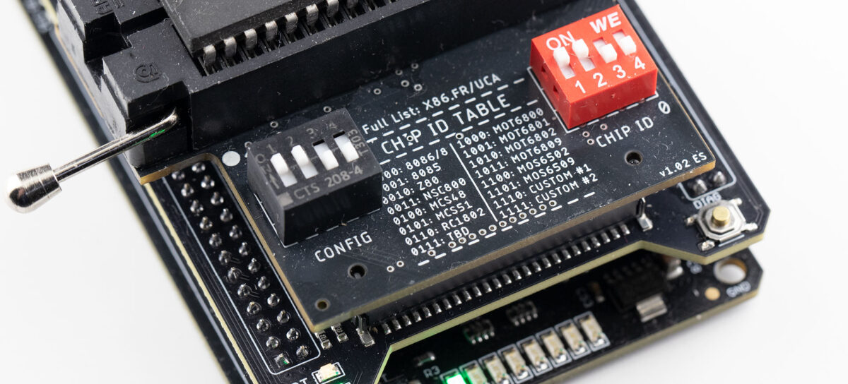
The DIP40 Adapter has a 4-way dip switch to select the CPU under test between the following:
Intel 8086/8088
Intel 8085
Zilog Z80
National Semiconductor NSC800
MCS-48 (80C48)
MCS-51 (8051)
RCA CDP1802 (COSMAC)
Intel 8087 (Work in progress)
Motorola 6800
Motorola 6801
Motorola 6802
Motorola 6809
MOS 6502
MOS 6510 (or MOS6509, still TBD, would like your opinion!)
All these CPUs are now supported by the DIP40 Adapter directly! This should cover 95% of the most common CPUs that came in DIP40. What about more obscure ones? If you zoom in on the picture above, you can see that two positions of the configuration switch are marked “CUSTOM #1” and “CUSTOM #2”. Users will be able to upload any other firmware to these two slots. For example, CPUs like the Motorola 6809E or the Ricoh 2A03 can be added in the custom slots when they become available. Basically, any CPU with VCC on pins 5, 6, 7, 8, 11, and/or 40, and GND on pins 1, 20, 21, and/or 29 can be supported. Some niche CPUs like the Signetics 2650 or the Intersil 6100 (which have vastly different pinouts compared to all other CPUs) will still need a custom adapter, but the new DIP40 Adapter alone should be enough for almost everyone out of the box, from pinball enthusiasts to retro researchers.
![[VIA’s Graveyard] Exhuming the VT5329E (PN133 Development Board)](https://x86.fr/wp-content/uploads/2026/06/VT5329E-BANNER-1200x540.jpg)
 The is significantly larger than a standard motherboard and will not fit in a conventional ATX case. This is confirmed by the unusual placement of the audio jacks, which are aligned with the PCI slots and would prevent the board from being mounted properly. The board has 3x SDRAM, 2x PCI, 1x ISA and 1x AMR slots, and is based on the VT8603 (“Twister”) Northbridge, the first VIA Northbridge to use a S3 integrated chipset instead of the previous Trident IGP.
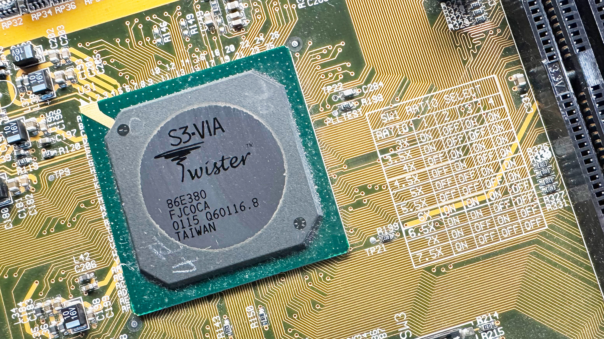 Between 1998 and 2002, VIA’s Socket 370 chipset lineup became rather confusing, with numerous renamings and rebrandings over that five-year period. All VIA Socket 370 IGP northbridges internally use the VIA Apollo Pro 133, or Apollo Pro 133A, northbridge combined with a third-party graphics core. As a reminder, the main difference between the Apollo Pro 133 (VT82C693A) and the later Apollo Pro 133A (VT82C694X) is that the latter adds support for AGP 4X. Both supports FSB 66/100/133 and SDRAM PC133.
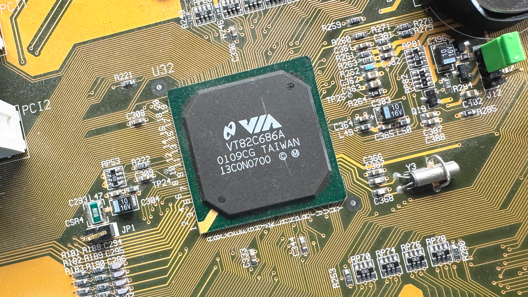 There are not many differences between the 686A and 686B. The latter basically just adds ATA100 (UDMA 5) support. Both supports PCI-to-ISA bridge, AC’97 audio, an integrated Super I/O chip with monitoring, SMBUS and USB 1.1 (up to 4x ports). On the VT5329E, it seems clear that the audio codec part was specifically targeted for evaluation.
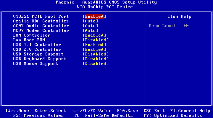
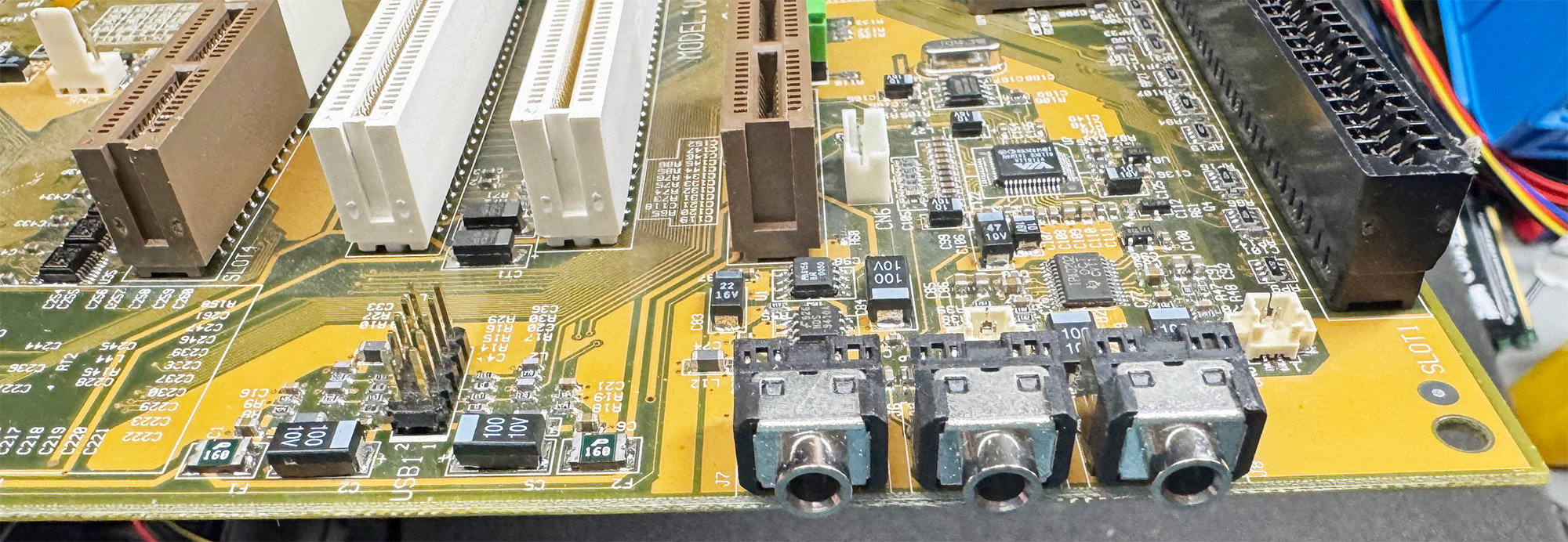 The board has jumpers for AC’97 (provided by a VT1611A), MC’97 (modem counterpart), AC’97+MC’97 and for the dedicated audio/modem codec slot (AMR). Note that this is the older (circa 1998) AMR specification and not the newer CNR standard that was introduced by Intel in 2000.A very interesting point is the strange slot located close to the Northbridge
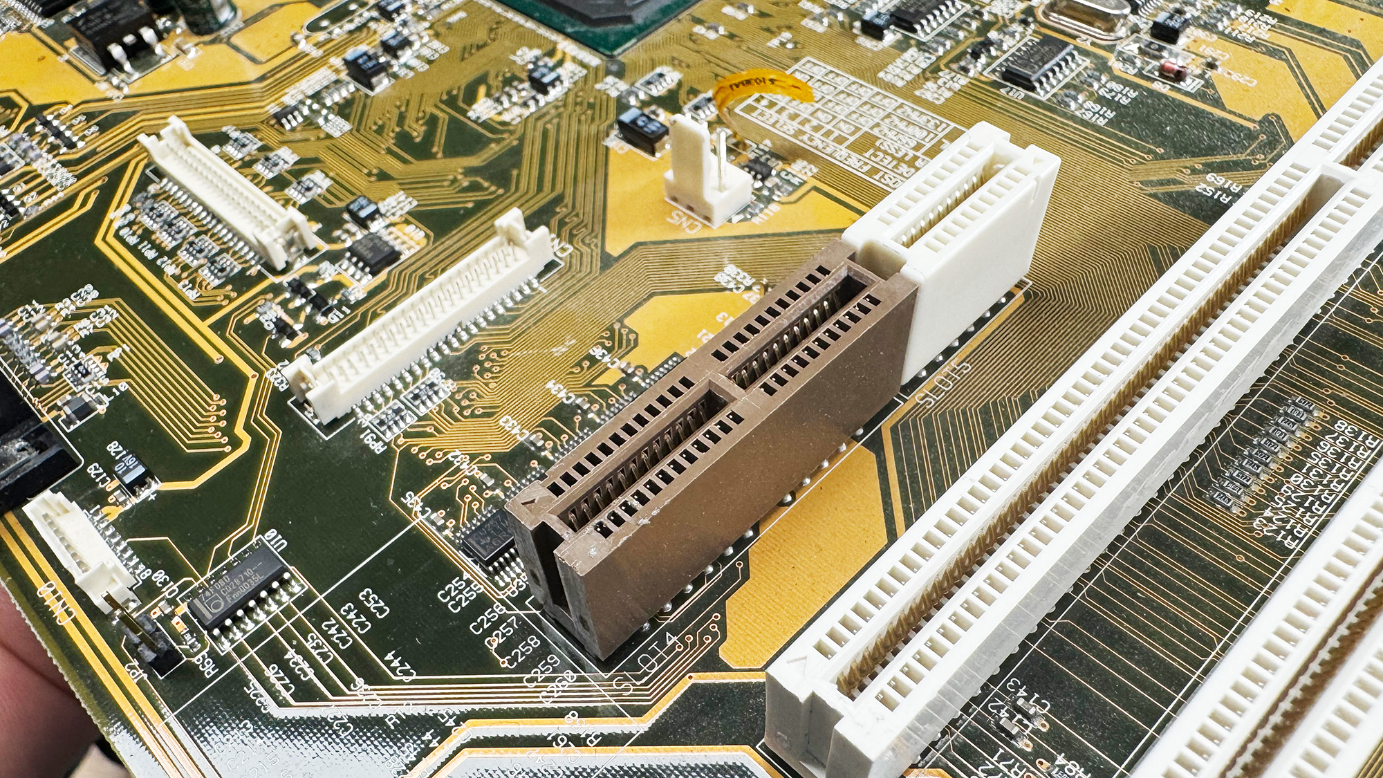 Physically, it resembles an AMR slot with a small white extension similar to the end of a PCI slot. Electrically, however, it has nothing to do with AMR. Based on the PCB traces and the voltage translators located nearby, my best guess is that this slot breaks out the LCD panel signals for debugging purposes.
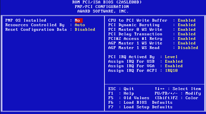
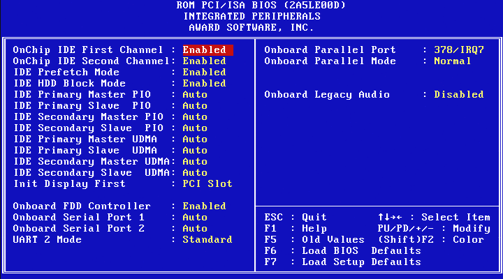
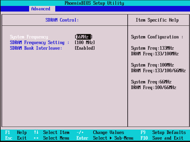
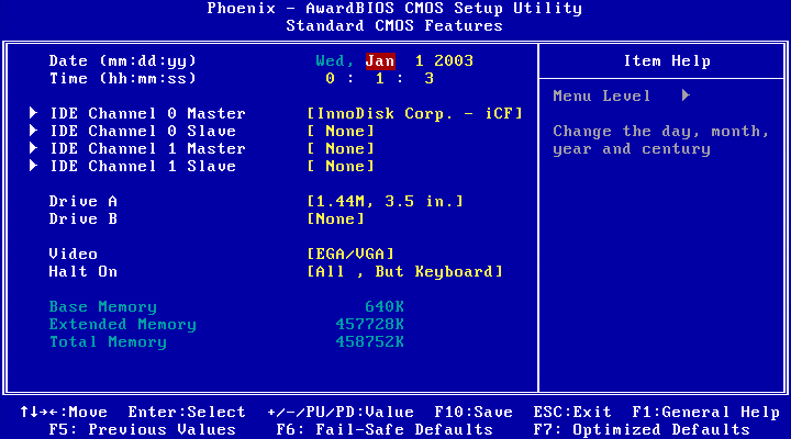
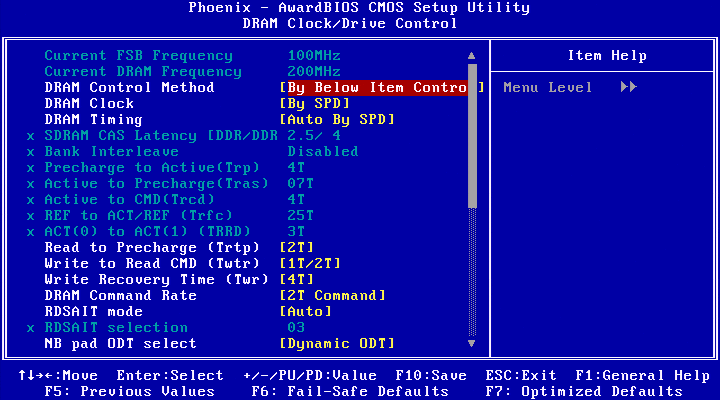
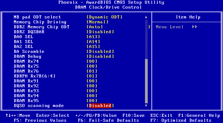
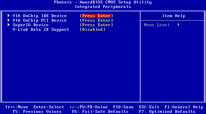
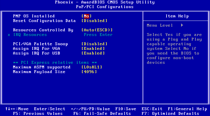
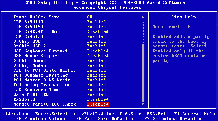
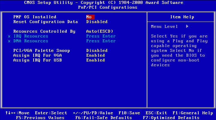
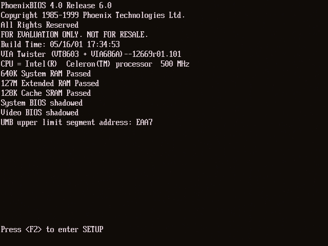 We are greeted by a Phoenix BIOS 4.0 instead of the usual Award 6.00 BIOS. Not really surprising for a Mobile development platform (Phoenix BIOS were much more common in laptop). The boot strings include “FOR EVALUATION ONLY. NOT FOR RESALE” and “VIA Twister (VT8603 + VIA686A) –12669r01.101” with a build date on 2001-05-16. The configuration menu is quite nice:
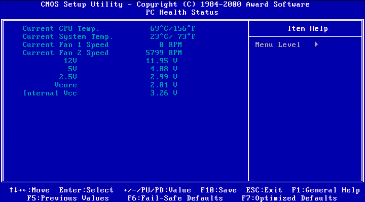
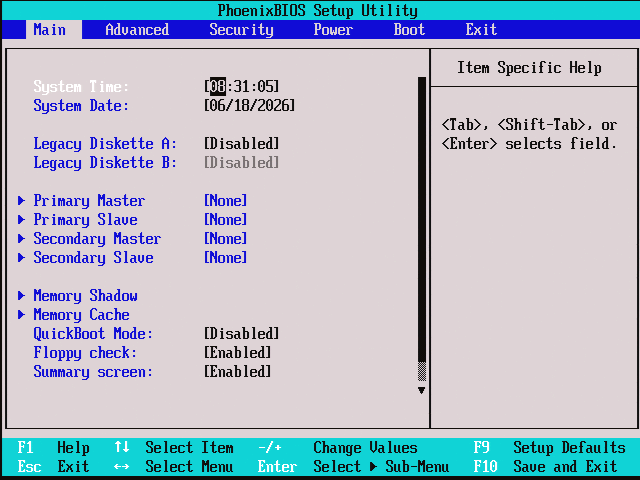
![[VIA’s Graveyard] Reviving the VT5910A (Early C7-M + Unknown CN900 chipset)](https://x86.fr/wp-content/uploads/2026/06/VT5910A_banner-1-1200x482.jpg)
![[VIA’s Graveyard] Autopsy of the VT5426D (First step to Mini-ITX!)](https://x86.fr/wp-content/uploads/2026/05/VT5426D_BANNER.png)
![[VIA’s Graveyard] Booting the VT5292A (Apollo PLE133 Reference Board)](https://x86.fr/wp-content/uploads/2026/05/VT5292_BANNER-1200x532.jpg)

![[VIA’s Graveyard] Resurrecting the VT5182E (Apollo MVP4 Reference Board)](https://x86.fr/wp-content/uploads/2026/05/VT5182E_06-1200x675.jpg)