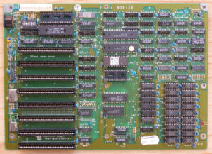
The Universal Chip Analyzer was not called the Universal CPU Analyzer for a reason: from the very beginning of the project back in 2017, I have in mind a tester for various ICs and not just CPUs. The 8087 was the first non-CPU that could be tested on the UCA, but a FPU is technically close to CPU. Another component that often fail on early 70s & 80s computers is the memory (“RAM”) chips. Back in these days, DRAM didn’t come in SIMM or DIMM modules like in the 90s and later, but simply as individual ICs assembled on the motherboard. The most common were the 2164/4164 (64 Kbits) and the 21256/41256 (256 Kbits) as found on the original IBM PC XT motherboard or many other iconic computers like the Commodore 64. Below, a motherboard from a DTK PC clone featuring 18x 41256s in the bottom-right corner totalizing 576 KB of raw memory (512 KB useable).
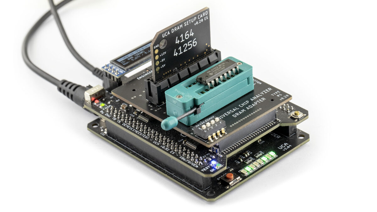
There is a LOT of different DRAM chips from that era, so I had to build an almost universal DRAM shield, able to supply all the common voltages (+5V, -5V and +12V). I choose a universal DIP20 ZIF socket that should cover almost all the 1-bit and 4-bit wide DRAM used in these computers. Unfortunately, an almost infinite variety of pinout existed back then. The easiest solution to route the correct signals to their appropriate pins was to add dedicated “Setup cards”, one for each different pinout. PCBs are cheap these days and these setup cards only use 2-layer PCBs, costing less than $2 each. The type of card inserted is of course automatically detected by the UCA. I started with the 2164/4164 and 21/41256 (1-bit wide DRAMs).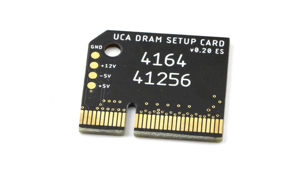 For the first proof of concept, I used a standard PCI Express 4x connector. I’m not totally happy with this connector because it requires the plugged-in card to be perfectly perpendicular to ensure a perfect electrical connection. In the other end, it’s also very convenient and easy to use. I successfully tested many different 2164, 4164, 21256 and 41256 chips, as well as other DRAMs that use the same pinout (like IMS2600).
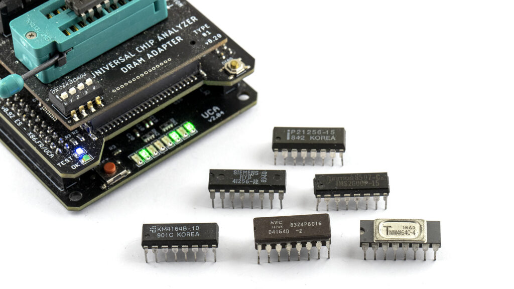 The test routine run by the FPGA includes checking for stuck 0s, stuck 1s and adjacent bits flipping correctly from 0 to 1 and from 1 to 0. I have also added more advanced tests (thanks to the years spent on Memtest86+) like memory retention between refreshes, which can degrade over time. The firmware can detect any errors and report the memory address that failed. It can also detect if the DRAM chip supports advanced features like paging (subsequent column access without toggling RAS) and the obscure nibble mode (a limited paging access).
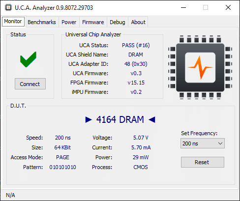 One of the most interesting features of the UCA is the ability to test DRAMs at their rated speed. A chip originally rated at 150 ns access time can now be limited to 200 ns due to aging for example. I have added 100 ns, 120 ns, 150 ns and 200 ns as standard access time but other frequencies are possible as well. Of course, the current and power consumption of the chip is measured. I’m also thinking about more settings like the refresh time. Here is a logic analyzer dump of the standard test process right now:
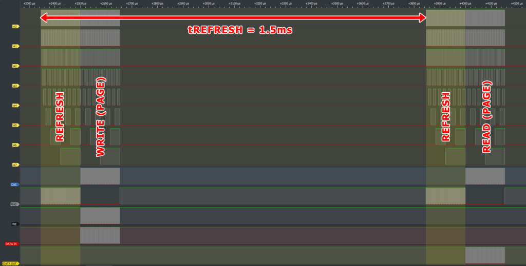 I use a 1.5 ms (1500 µs) delay between refreshes because it’s the shortest allowed by some ICs according to their datasheets, but more advanced DRAMs support “Extended Refresh time” that allow up to 4 ms between refreshes without data loss. Adding customizable tREFRESH delay can be helpful in the future. Also, I will build a new UCA™ Setup Card© for 4116 as they were very common in late 70s computer like the Apple II. They need a specific card because they require -5V and +12V instead of the single +5V supply of later 4164 & 41256. 4-bit wide DRAMs like the 4464 and 44256 will probably follow soon.
Feel free to suggest any different DRAM (with max 20 pins) from that era!

