If you’ve been following my blog since the inception of the Universal Chip Analyzer (UCA) journey, you might recall a post with the same title I published in mid-2021. At that time, I was excited to unveil the second version of the UCA, a project I had been dedicated to since 2017. Unfortunately, shortly after this announcement, the integrated circuit (IC) industry faced a significant global shortage. This crisis led to exorbitant price hikes, severely impacting the production of the UCA’s initial batch. In 2022, I made a pivotal decision to entirely overhaul the UCA project, encompassing both its hardware and software components.
Initially, I questioned the necessity of upgrading beyond the original components, a Xilinx Spartan-6 FPGA and a Cortex-M0 based microcontroller (MCU). These components seemed adequate for the previously stated applications. However, I’ve come to realize the immense benefits of this upgrade. The rationale behind the UCA’s redesign is twofold: versatility and longevity. By incorporating more powerful components, the UCA’s capabilities have been greatly enhanced, truly living up to its “Universal” moniker. This complete modular redesign not only broadens its applications in retro-computing beyond mere component testing but also incorporates every feature I envisioned without the constraints of the original Mojo development platform.
This latest iteration, internally referred to as “v3,” marks a significant evolution from its predecessors. The UCA v1 was a modification of the Mojo v3 from Alchitry, featuring custom firmware and an upgraded Flash chip. The UCA v2 introduced a superior Cortex-M0 based MCU while maintaining the core architecture of the Xilinx Spartan-6 FPGA. Below is an image showing the progression from v1 (right) to v2 (middle), leading up to the latest v3 (left):
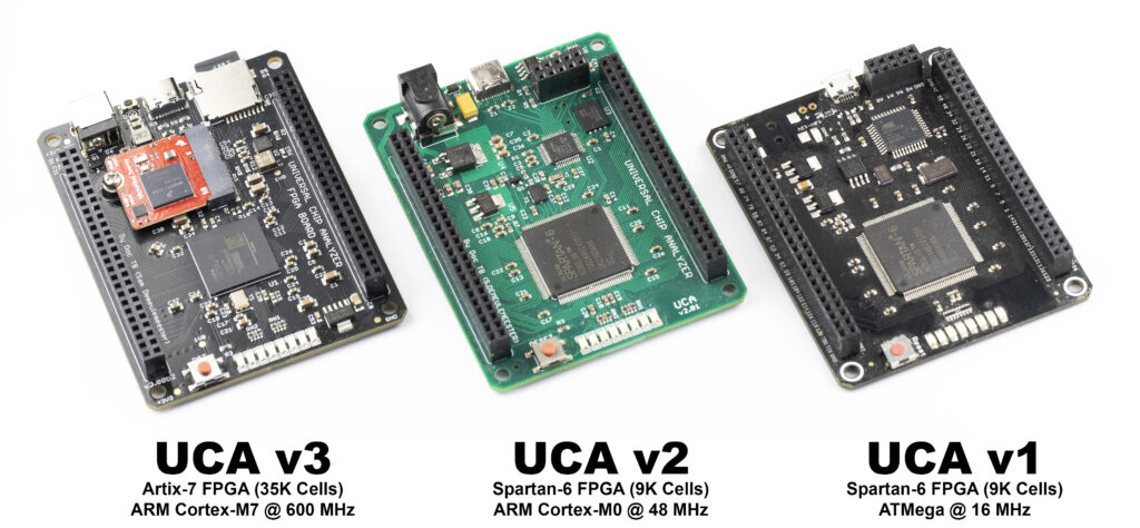 UCA v3 Hardware
Let’s delve into the specifics of the final version of the Universal Chip Analyzer (UCA).
-
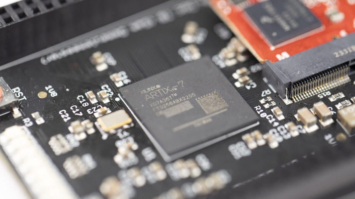
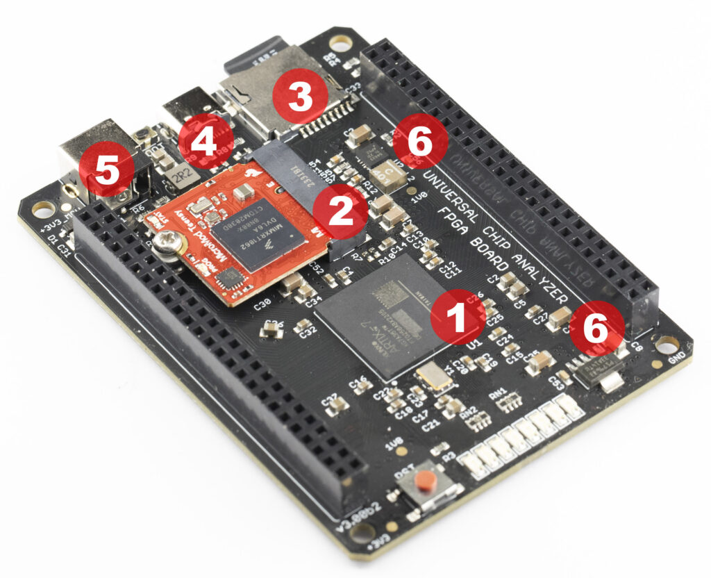
- FPGA Upgrade – The most notable enhancement in the UCA v3 is the transition from a Spartan-6 to an Artix-7 FPGA. The original Spartan-6 XC6SXL9, a 45nm FPGA, featured 9,152 logic cells and 576 Kb of Block RAM. In stark contrast, the Artix-7 XC7A35T, fabricated on a more advanced 25nm process, boasts 33,280 logic cells and 1.8 Mbit of Block RAM. This represents a threefold increase in size, coupled with improved power efficiency and additional features like an integrated ADC. Despite being available only in BGA packaging, soldering the Artix-7 proved to be surprisingly manageable.
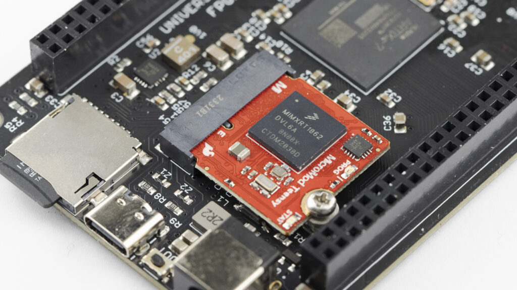
- Microcontroller Unit (MCU) – The MCU plays a crucial role in the UCA, responsible for loading the appropriate FPGA firmware, facilitating communication between the FPGA and external devices via USB, managing integrated voltage regulators and their safety protocols, displaying information on the OLED screen, and handling various auxiliary tasks. The MicroMod Teensy, a collaboration between Sparkfun and PCJR, was selected for its ease of use, impressive power, and open-source status. Based on the NXP i.MX RT1062 microcontroller (ARM Cortex-M7 @ 600 MHz), it includes 1024K RAM, 16MB Flash, and supports an extensive range of peripherals. Its integration into the MicroMod ecosystem means it’s housed on a small, replaceable board with a standard pinout and a common M.2 connector. This not only simplifies the design but also reduces costs and facilitates future upgrades if needed.
- MicroSD Card Integration – The UCA operates on various FPGA configuration files, known as bitfiles, with each hardware configuration requiring a specific bitfile. Earlier versions used a 256 Mbit (64 MB) SPI Flash IC, limiting the storage to about 100 configurations. To accommodate the larger bitfiles required by the Artix-7 FPGA, which are over 2 MB, a MicroSD card was introduced. This solution offers practically unlimited storage and, thanks to the performance capabilities of the new MCU, enables quick firmware loading – a 2.2 MB firmware can be loaded in just 500 ms.
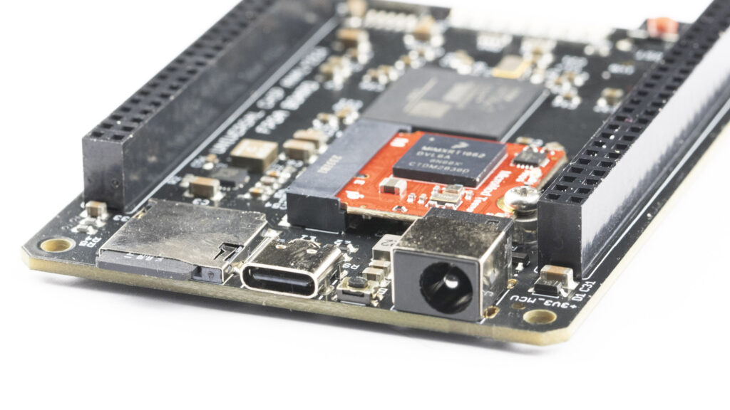
- USB-C Connectivity – First introduced in the UCA v2, the USB-C connector continues to facilitate communication with the companion app for advanced testing and monitoring. The enhanced NXP i.MX RT1062 MCU paves the way for future feature expansions.
- DC connector – The inclusion of a standard 2.1mm low profile DC connector is essential for powering the adjustable DC-DC voltage regulator on the Interface (IF) board with a 9V to 12V power source. This is particularly crucial for powering newer CPUs like the 486 DX2/DX4. Two versions of the IF board are planned: a fully-featured variant supporting a wide range of voltages and a simplified version for testing 5V ICs without the need for external DC power.
- Enhanced Power Regulators – The shift to the Artix-7 FPGA necessitated a complete overhaul of the UCA’s power management system, given its more complex power requirements compared to the Spartan-6. The board now incorporates two DC-DC switching regulators (one for the main 1.0V FPGA core voltage and another for the 3.3V MCU) and two linear converters (one for the 1.8V FPGA auxiliary voltage, and another as a low-noise converter for 3.3V I/O).
- FPGA Upgrade – The most notable enhancement in the UCA v3 is the transition from a Spartan-6 to an Artix-7 FPGA. The original Spartan-6 XC6SXL9, a 45nm FPGA, featured 9,152 logic cells and 576 Kb of Block RAM. In stark contrast, the Artix-7 XC7A35T, fabricated on a more advanced 25nm process, boasts 33,280 logic cells and 1.8 Mbit of Block RAM. This represents a threefold increase in size, coupled with improved power efficiency and additional features like an integrated ADC. Despite being available only in BGA packaging, soldering the Artix-7 proved to be surprisingly manageable.
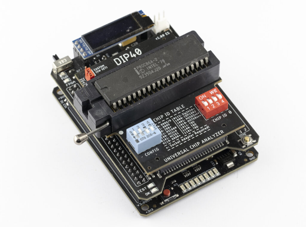
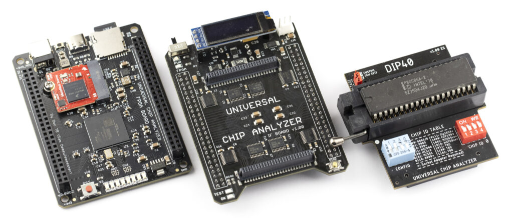 Despite these significant upgrades, the UCA retains its compact dimensions (85×63 mm), similar to a credit card, and continues to be based on a mezzanine stack design. The first layer is the FPGA board (as described), followed by the Interface (IF) Board, which integrates the OLED display, DUT (Device Under Test) power management, and signal conversion. The final layer is the Adapter Board, equipped with a socket suitable for a specific type of chip (CPU, DRAM, etc.).
Here’s a glimpse of the complete UCA v3 with the DIP40 Adapter Board:
 UCA v3 Software
From a software perspective, the transition from the Spartan-6 to the Artix-7 FPGA in the UCA v3 brings substantial advantages. Let’s delve into some of the key developments in the FPGA domain. Xilinx, now part of AMD, recently extended the lifespan of the Spartan-6 series to at least 2030. This sounds promising, but there’s a significant caveat: Xilinx discontinued their 6-Series FPGA toolchain and development tools, known as Xilinx ISE, back in … 2013! As a result, anyone looking to code for a Xilinx 6-Series FPGA today is forced to use an outdated, bug-ridden tool that lacks support for modern operating systems like Windows 10. The only viable workaround is running the tool on an old Linux VM. To put it bluntly, working with ISE in 2024 is a nightmare.
The shift to a 7-Series FPGA like the Artix-7, on the other hand, enables the use of Xilinx’s current “Vivado” toolchain, which is under active maintenance. This change is significant. When I initially embarked on the UCA project in 2018, the learning curve was steep, and I relied heavily on Xilinx 6-Series specific primitives and IPs for simplicity. With the move to the Artix-7, I made a strategic decision to rewrite everything in pure (System)Verilog, minimizing the use of specific IPs. This approach not only facilitates future transitions to different FPGA brands or models if necessary, but it also allows for the release of all the code as open-source software.
What’s Next?
The immediate objective is to finalize the UCA v3 hardware validation as quickly as possible. My aim is to ensure the FPGA and IF boards won’t require further modifications for years, allowing me to concentrate on software development, adapter creation, and other innovative features. The initial focus will be on beta testing the DIP40 and 486 adapters. If the UCA v3 successfully runs a 486 DX4 and an 8080, like the UCA v2, I’m confident that the hardware will be robust enough for any CPU released in the 70s, 80s, and up to the mid-90s.
The Universal Chip Analyzer v3 will be available for sale soon, starting with the DIP40 adapter. Subsequent adapters will then be released one-by-one. Pricing details will be announced in the near future. While I’m considering another Kickstarter campaign, akin to my experience with the ATX2AT Smart Converter, I’m mindful of the significant time investment such crowdfunding efforts entail.
Stay tuned for more updates on the UCA, and feel free to share your thoughts and comments!

Grande lavoro ! Complimenti
Bonjour,Super projet. Le projet est il en vente? Si oui a quel prix? Qui le distribue? Prix des accessoires adaptateur dip 40 insertion nulle?merci
Bonjour. L’UCA V3 est en cours de beta test final actuellement. Le prix sera annoncé bientôt.
Does the v3 hardware help with supporting higher-frequency buses?
50MHz bus: Intel/Cyrix 486DX at 1x50MHz; Intel 486DX4 at 2x50MHz or 3x50MHz? (per Wikipedia: “Certain steppings of the DX4 also officially supported 50 MHz bus”); AMD 486DX5 at 3x50MHz and overclocked 4x50MHz; Cyrix 5×86 overclocked 3x50MHz
66MHz bus: per Wikipedia: “Some late model Socket 3 motherboards unofficially supported FSB speeds up to 66MHz” (there is a Cx486 SoC that supports it: http://www.zfmicro.com/library/manuals/ZFx86_Data_Book.pdf page 451), so: AMD 486DX5 at 1x66MHz, 3x66MHz (is it possible to run it at 2x multiplier?); Cyrix/ST 486DX4 at 1x66MHz, 2x66MHz; Cyrix 5×86 at 1x66MHz, 2x66MHz; maybe even Intel/UMC?
Yes, but frequencies higher than 40 MHz will require another shield (significantly more expensive) or adding wait states to the memory bus.
The UCA itself has been tested successfully up to 80 MHz bus.
Do you know if RDC R321x (386, http://d1.nuuo.com/NUUO/IO_POS/IO%20Box/Prohubs/R3210_F13_LQFP_full_%2020080828(Gigabyte).pdf) or R86xx (486SX, http://www.sima.com.tw/download/R8610_D06_20051003.pdf) have CPUID?
– RDC: 8051 (1998), 186 (2001), 386 (2004), 486SX (2007, used in Vortex86SX)
Other exotic chips:
– Intel: 8008, IBM486SLC/DLC, i486DX2 P24LM 90/30 MHz (per Wikipedia; odd due to triple-clocked DX2 and frequency), i486GX (16-bit data bus)
– others: VM386 (1988, VM Technology), VA186 (2000, VAutomation), IA186 (2005, InnovASIC)
– FPUs: 287/387 variants (IIT, ULSI, LC, C&T, etc.); NEC μPD72091, μPD72191/D9008D, 72291; Am9511/i8231, Am9512/i8232; Weitek FPUs; Cyrix 8087, Cx487S (not a 486DX, but actual co-processor for Cx486S); Nx587
Can UCA Analyzer be made to show also if the chip supports:
– MSR (for IBM386/486)
– C&T SCALL “CPUID-like” result
– System Management Mode for non-486 CPUs (currently SL/SMI is shown only in the 80486 tab): SMI/SMM/RSM/SL for i386SL, IBM386 and some Am386; their own implementations for C&T (186, 386), ALi, NexGen
– 386 “CPUID” reset value of EDX for 486 and later CPUs (currently it’s shown only for 386-bus chips? it’s not the same as CPUID EAX which shows FamilyModelStepping instead of various combinations of FamilyModelRevision/ModelFamilyRevision/etc. for the reset value? CPUID Stepping and Reset-EDX Revision show different things for some CPUs? see https://github.com/joncampbell123/dosbox-x/discussions/4967#discussioncomment-9451050 – maybe label that “EDXID”, “ID” or “ResetID” instead of CPUID)
– bus width for non-486 CPUs (address 14/16/20/24/26 (i386EX/CX)/29 (VM Technology)/32-bit, data 8/16/32-bit, multiplexed or not); bus frequency for Cx486SLC/DLC can be inferred if the user calculates frequency/multiplier, but maybe can also be shown directly
– VME, PSE – although those are already shown via the CPUID EDX result (e.g. 0xB for i486DX4, thus showing that both are supported)
– there are various obscure instructions not supported by all CPUs https://github.com/joncampbell123/dosbox-x/discussions/4967
…and if you go beyond currently supported CPUs:
– which of the instructions added in 486 (CMPXCHG, BSWAP, XADD, INVLPG, INVD, WBINVD) – for example NexGen supports only CMPXCHG, BSWAP, XADD https://www.cpu-world.com/forum/viewtopic.php?p=189409
– features added after Pentium, but without CPUID bit: RDPMC, Long NOP
As user have full control on any hardware and software part of the CPU, everything can be tested.
Reset “CPUID” Value are already logged and various specific MSRs are used.