IBM 386
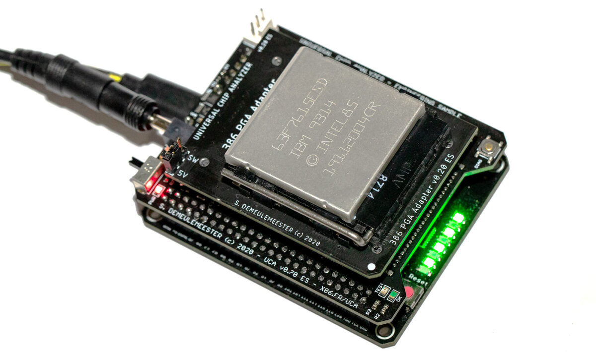
As like all previous microprocessors, Intel licensed the i386 design to third parties. AMD was the only one legally allowed to sell Intel-based 386s to customers (as bare CPUs), but IBM was granted the right to produce some Intel 386s for its own use. They don’t look like a standard ceramic CPUs : IBM used a plastic substrate and a metal cover to protect the die and help with thermal dissipation. Here is how they look like.
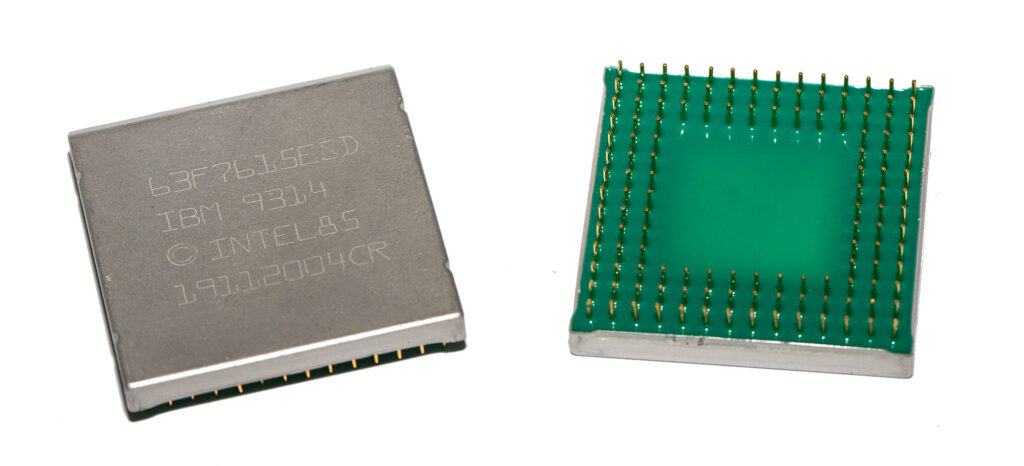 If the packaging is different, the internal die is the same as on Intel 386s. 7 different IBM part-numbers are actually known: 23F7189 (?? MHz), 32G6633 (25 MHz), 51F0352 (20 MHz), 51F1783 (20? MHz), 51F1784 (20 MHz), 51F1797 (25 MHz) and 63F7615 (25 MHz).I was able to put my hand on a 51F1784 and the later 63F7615. I tested both on the Universal Chip Analyzer. There is no “Pin 1” mark so I had to guess where is pin 1. Fortunately, the UCA has strong over-current and short-circuit protection. Let’s start with the 63F7615 :
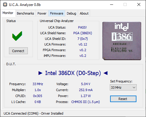
This one is able to work fine up to 33 MHz, with a CPUID set at 0x305, similar to Intel 386 based on the D0-stepping. I don’t know for sure the real rated frequency, but it’s probably only 25 MHz. The other one (51F1784ESD) is not able to work at 33 MHz and not even at 25 MHz. The actual (early) UCA firmware only has 16/25/33/40 MHz, so I can only confirm that that my 51F1784ESD works at 16 MHz but not at 25 MHz. According to various sources, it’s probably rated at 20 MHz.
AMD Am386
AMD also produced a lot of Am386DX at 20, 25, 33 and 40 MHz. While the microcode is 100% from Intel, the manufacturing process is different and they had lower power consumption (thanks to the 0.8µm process used by AMD instead of Intel’s 1µm CMOS-IV on the latest i386s).
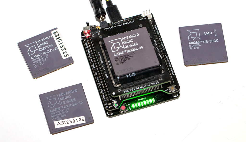 Let’s start with the standard Am386 DX/DXL. I tested one Am386 DX/DXL-25 “B-Step”, one Am386 DX/DXL-33 “D-Step” and another Am386 DX/DXL-40 “C-Step”. All came in the 23936 package from Kyocera.
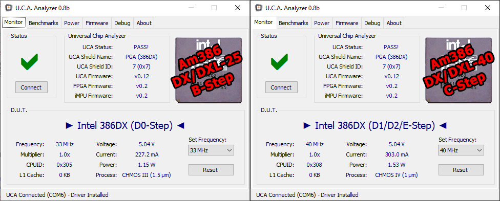 The UCA tool is not yet able to detect them as AMD, but I’m working on a new algorithm based on power consumption to distinguish them from Intel 386s. The B-Step identifies itself as 0x305, the same CPUID used on Intel’s 386 D0-Step. The DXL-25 was able to work up to 33 MHz. Both C- and D-Step have a CPUID set at 0x308, like the later Intel 386s (D1 step and up).
The last CPU to try was the Am386DE-33, an uncommon embedded model. Like the Am386DXL, it uses a fully-static design, meaning it can be clocked down to DC (0 Hz) while retaining all its internal registers content. The biggest difference between the usual Am386DX/DXL and the Am386DE is the disabled Paging Unit in protected mode on the latter. Bit 31 of CR0 (used to enable paging) is reserved on Am386DE. Another difference only available on the Am386DE is the ability to work at its rated frequency with a much lower voltage (down to 3.0V). And it works fine:
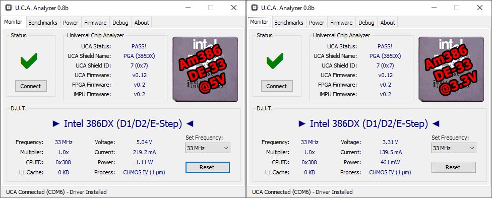 At 3.3V, the power needed drops by a huge margin, from 1.1 Watt to as low as 461 mW (0.46W). That’s a -60% power reduction!

Do you have any information or knowledge about what AM386 chip is used in the BEHRINGER DANALOG DDX3216. I noticed that this is likely the main system CPU an AM386, that connects to an EPROM that holds the firmware and a coderdecoder. There is 16mb of flash memory and 16mb of ram both being 8indivudal chips of 2mb or something like that, then there is likely some type of DSP out to the sharc processor. The PCMNIA and a disk controller chip is used. I am really curious if the AT keyboard and CGA pins on the AM386 might be able to be used to provide a video output and keyobard control of the ddx3216.. also curious if AT keyboard signals might be send via the midi MMC rs232 cable. I was thinking maybe the at keyboard cpu functions were used to map buttons etc.. not 100% sure yet but getting more information on this chip may help me better underestand if something like DOS could ever be run, perahps using the PMCIA port as some type of harddrive of sorts as the LCD screen alone is probably more time consuming to navigate than what could be done with a CGA monitor and keyboard… as a control interface. Long term project but it seems you are pretty knowledgable about the x86 architecture these chips are based on and it seems that this is the architecture that is being used to control the digital mixer. I would like to access the sharc DSP and I am thinking that altering how the fxs are stored / processed by unlocking the cpu and putting an os that can house the firmware itself might expand the function of the mixer — lot of work but its basically a computer as far as I understand with ram/rom a cpu a dsp sharc processor and a flash bios of sorts in the form of firmware on an emprom with BIOS decoder/coder chip, and PMCIA port in place of a disk drive… seems like it might be possible.
I fear that this is a bit off topic as doing anything like this requires a deep knowledge of the device architecture. An x86 CPU can be used without any form of operating system, just as a DSP.
Per https://en.wikipedia.org/wiki/IBM_386SLC#IBM_486SLC there are also IBM 486SLC/DLC
– Intel 486 with 386SX/DX bus, up to 3x33MHz
– 100-pin BQFP / 132-pin QFP
– they support SL/SMI, MSR (https://web.archive.org/web/20040604002243/http://debs.future.easyspace.com/Programming/OS/cpuid.txt)
– maybe support CPUID (some of them are released after Pentium)
Non-PGA/PLCC/LGA CPUs are much harder to physically test on the UCA because they need a specific Test Socket.
For QFP 486SLC/DLC, Test Socket are usually very expensive ($100+).