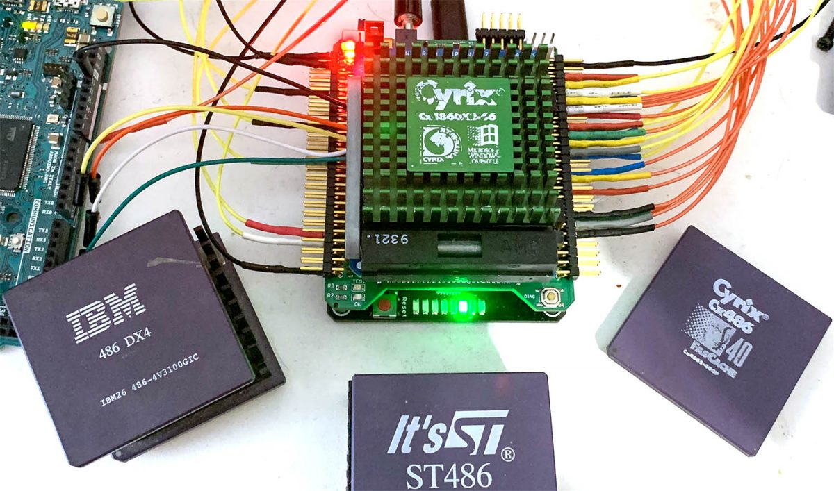
Along with AMD, Cyrix was one of the biggest Intel challengers in the 486 era. While most of the AMD Am486s used the exact same microcode as Intel 486s, Cyrix was the first to release a 100% compatible processor based on a custom design. Being a fabless company, Cx486s were manufactured by IBM, ST Microelectronics and Texas Instruments. All of them sold Cyrix 486s under their own brand.
Adding support for Cyrix-based 486 and 586 was more challenging than expected. As many of you probably remember, 486 motherboards were full of jumpers because of the many different pinouts. I want the UCA to be able to test every CPU out of the box without messing with jumpers, so I had to use many tricks to accommodate the different pinouts. I also wasted a lot of time trying to understand the erratic bugs I had when adding more x86 code to detect Cyrix CPU. The cause was finally obvious, but I had a hard time spotting it: two address lines (A11 & A9) had been inverted in the FPGA code for more than one year!
This stupid typo came on top of another Cyrix-only specification I had to deal with. All the HDL code I wrote for the UCA is focused on achieving 0 wait-states. Unfortunately, when I started to work on support for the Cx486, it crashed almost instantly, even at low frequencies. I rewrote a lot of Verilog to achieve near-perfect timing, matching the original Intel datasheet almost perfectly. But the Cx486 kept crashing. I had to wire everything to my 32-channel logic analyzer to understand why all Cyrix 486s failed to work on the UCA. The answer is shown on this screenshot:
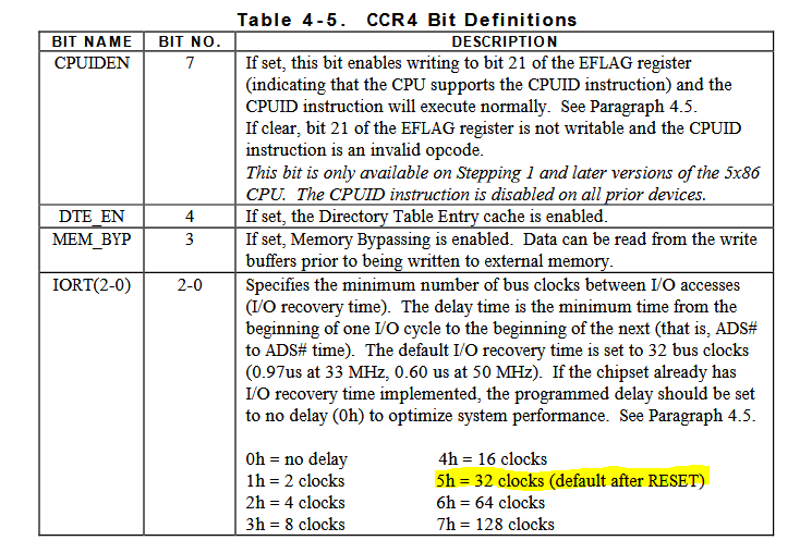
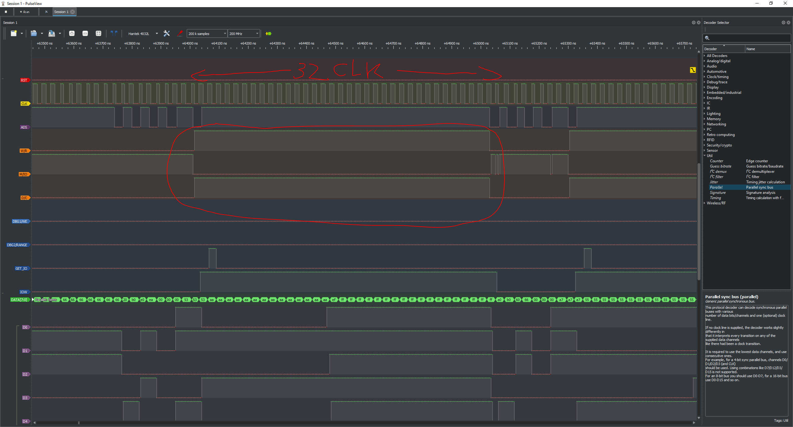 Cyrix added an unexpected (normally chipset-related) mechanism that adds hardware wait-states to every I/O. And not just a couple of them: 32 clock cycles for every I/O by default! The state machine that handles the decoding of CPU cycles inside the FPGA wasn’t able to understand why the CPU doesn’t resume operation after an I/O and assumes a timeout has happened. As soon as I changed the HDL code to handle this case, Cyrix CPUs started to work properly on the UCA. I could have saved myself a lot of effort if I had RTFM more carefully: this behavior is indeed described on the 5×86 CPU BIOS Writer’s Guide, page 12:
 Maybe I’ll add a software path later to change this setting with the UCA Analyzer tool. Messing with Cyrix-specific internal registers on the fly is an upcoming feature already planned! As with AMD, I grouped all the non-ES Cyrix CPUs I had in a tray and starts testing.
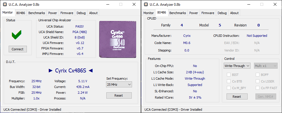
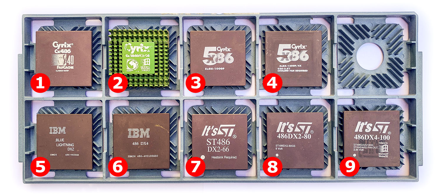 (1) Let’s start with the Cyrix Cx486S-40, one of the first 486-class CPU released by Cyrix in March 1993. It features 2 KB of write-back L1 cache, quite unusual for the time. The CPUID at reset is 0x450, which does not correspond to any Intel 486 (i486SX are 42x). Power consumption is quite high. Also note that the screenshot is done at 25 MHz for a rated maximum clock of 40 MHz. For an unknown reason that deserves a longer investigation, very early Cyrix 486 like this one cannot run at 33 MHz or more on the UCA with the actual HDL code. Maybe it’s due to the added electrical interference from the Logic Analyzer, or maybe It comes from a regression in the code after I messed with timings, but that Cx486S-40 was able to run at 40 MHz some days ago, so I’m quite confident It will be fixed soon. I was just too lazy to unwire everything to take the screenshot.
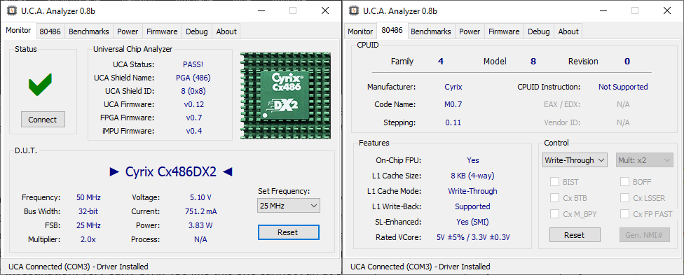
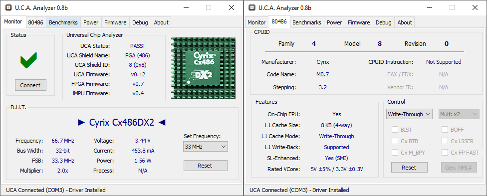
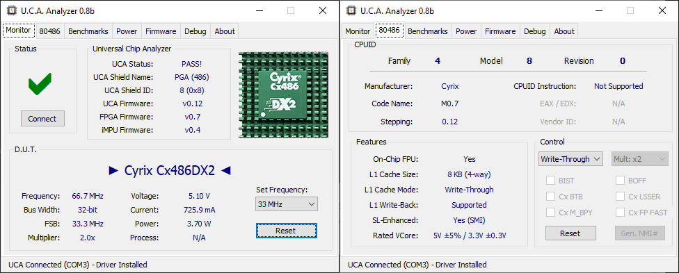
(2) Cyrix Cx486DX2-66. A clock doubled 486 with FPU. CPUID after reboot is 0x480 (similar to Intel DX4s) but the CPU does not support the cpuid instruction. Cyrix CPU has two registers named DIR0 and DIR1 for identification. This one contains 0x1B in DIR0, the hex value for a Cx486DX2. DIR1 contains 0x0B. DIR1[7:4] is “CPU Step Identification Number” (here 0x00) and DIR1[3:0] is “CPU Revision Identification” (here 0x0B or 11 in decimal). The actual “Cyrix stepping” is 0.11. This CPU is marked A3CM434M and has been manufactured week 34’1994. It’s an early example. Like the Cx486S, it does not work at more than 25 MHz on the UCA yet (but it will soon).
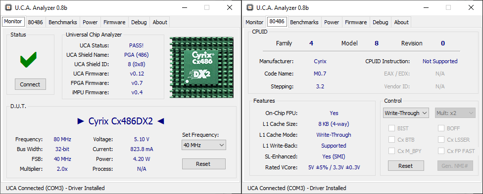
(5) IBM “Blue Lightning DX2” 486-V666GA. An IBM-branded Cyrix 486DX2-66. They are strictly identical from a microarchitectural point of view but are supposed to come with a stricter QC (Quality Control). This one is a 3.45-3.6V part, and not a 5V CPU like the previous one. It is also much newer (manufactured in March/April 1995). Stepping/Revision is 3.2. No problem running it on the Universal Chip Analyzer at 66 MHz (2 x 33.3 MHz).
(6) IBM 486 DX4 / 486-4V3100GIC. Well, I can’t remember where this CPU come from, but it doesn’t work. Not a single sign of life on the UCA not on a standard 486 motherboard. The power drawn seems linked to the clock signal applied (so the internal die is not shorted), but when wired to the logic analyzer, not a single pin toggles after reset. Unfortunately, it looks dead. 🙁
(7) It’s ST ST486 DX2-66. While IBM-branded Cx486s are often known for their higher QC (and higher overclocking), ST’s 486 are usually less overclockable. This CPU was manufactured in February 1995 but still uses the Stepping 0.12. A single step newer than the very old Cyrix Cx486DX2-66 but much older than the IBM Blue Lightning DX2. It works as expected at 66 MHz
 (8) It’s ST ST486 DX2-80. This part is very close to the IBM Blue Lightning DX2. It uses the same 3.2 Stepping but works at 5V instead of 3.45V. Power consumption is quite high (~4.5W) and it runs hot. CPUID is 0x480. No problem to have it running on the UCA at 80 MHz (2 x 40 MHz).
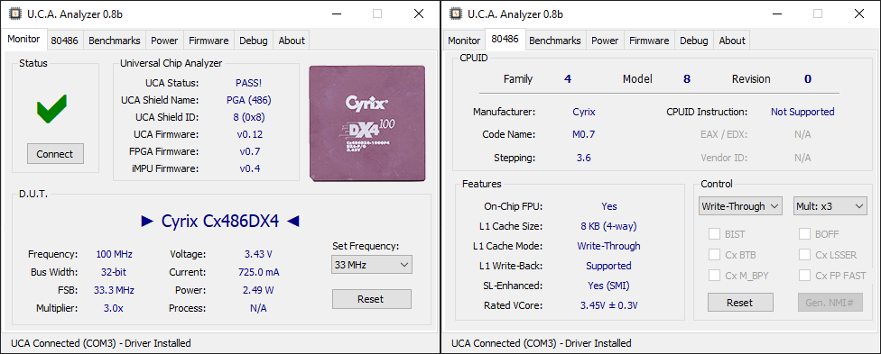
 (9) It’s ST ST486 DX4-100. Very late 3.45V clock-tripled CPU manufactured in 1997. The stepping is 3.6, which corresponds to the latest Cyrix 486 revision ever produced. CPUID is still 0x480 and L2 cache is limited to 8 KB Write-back (instead of 16KB for latest Intel 486 DX4s). It runs fine at 66 MHz (2×33.3 MHz) and 100 MHz (3×33.3 MHz).
(3) Cyrix 5×86-100GP. The 5×86 is a short-lived, stripped-down version of the Cyrix 6×86. It features 16 KB of L1 Write-Back cache and a 5th generation (Pentium class) microarchitecture. The vast majority of 5×86 processors run at 2x or 3x multipliers. This example is a quite early “1.3” revision. CPUID changes from 0x429 at 2x to 0x42D at 3x. It can work on the UCA at 120 MHz (3×40 MHz) with 3.6V.
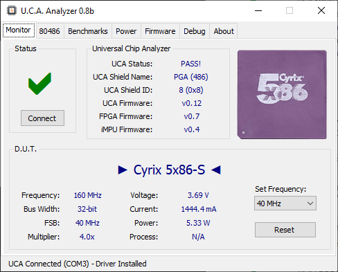
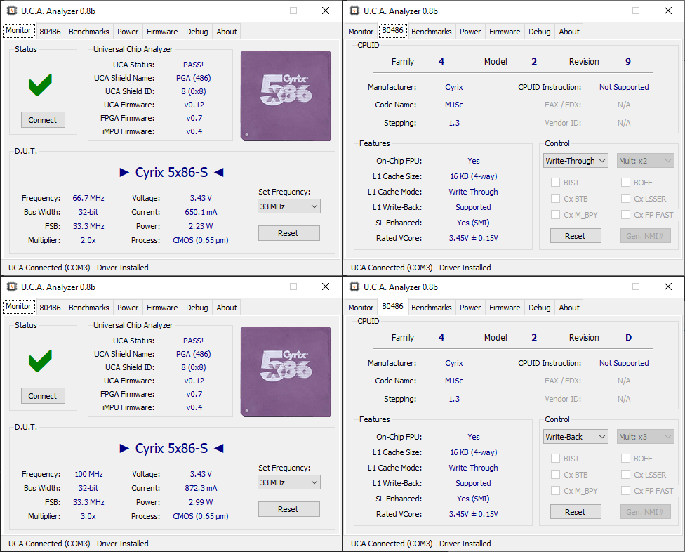 (4) Cyrix 5×86-120GP. Some late (and rare) 5x86s are able to work with a 4x multiplier (in addition to the default 3x multiplier). For some unknown reason, the revision/stepping drops to 0.5 even if the CPU was manufactured way after the previous one (in 1996). CPUID at 4x is 0x42C (and stay at 0x42D at 3x). Here is that nice 5×86-120 running at its rated 120 MHz (3×40 MHz) and then overclocked at 133 MHz (4×33.3 MHz) @ 3.6 volts
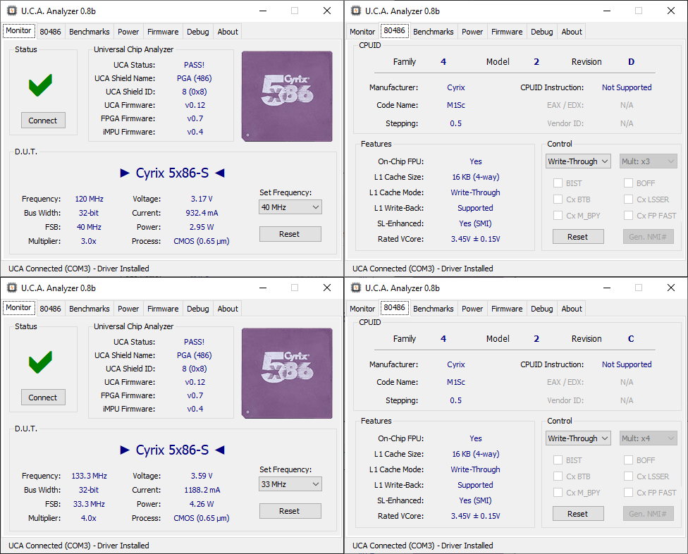 For fun, I also tried to increase the voltage to 3.7V before restarting the UCA at … 160 MHz (4x 40 Mhz) ! To my surprise, it successfully completed a test pass. I stopped to avoid any damage to the CPU, but that was probably the fastest pass ever run on the UCA.
 Awesome!
Next step is to add support for the remaining 486 brands (and solve the frequency regression on early Cx486s). I also have a nice feature upgrade for the 486 adapter planned soon. Stay tuned!
One thought on “The UCA 486 Adapter now supports Cyrix/IBM/ST 486s & 586s”
Comments are closed.