The UCA 386 Adapter now supports Intel RapidCAD

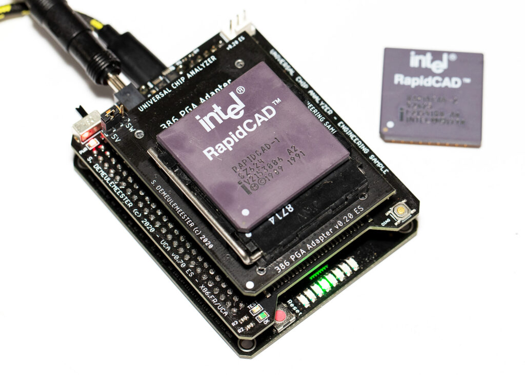
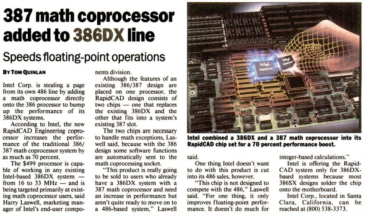
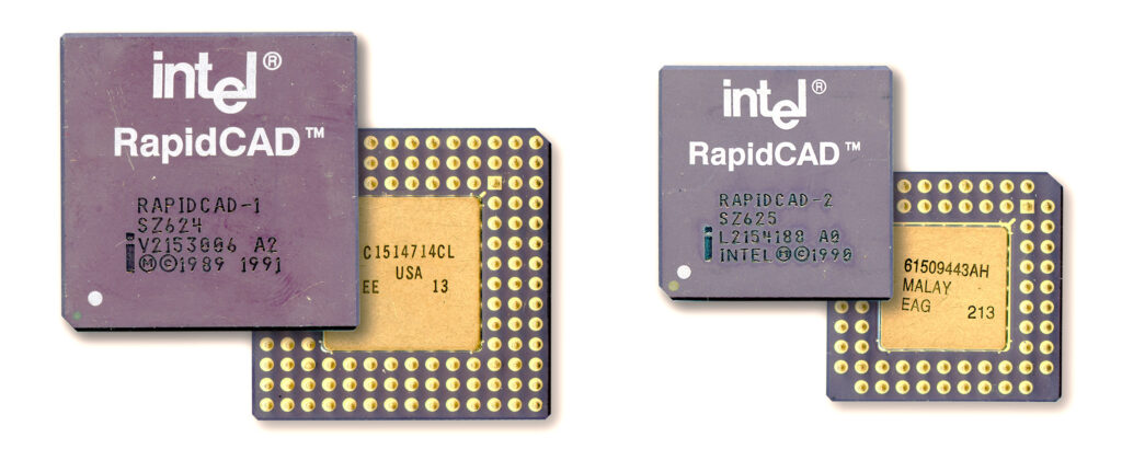
The elusive Intel RapidCAD Engineering CoProcessor is a weird and rare 2-chip set designed to upgrade 386 computers. It has been released in February 1992 for $499 and sold as a coprocessor. Technically, the RapidCAD is a 486DX assembled inside a 132-pin ceramic package that plugs into a standard 386 Socket. It features an integrated FPU but Intel removed the 8KB L1 cache and the 486-specific instructions. A second chip (RapidCAD-2) plugs into the 387 Socket, is only needed to provide the #FERR signal used to handle FPU exceptions.

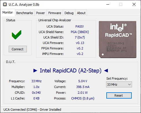
This early sample has been assembled in April 1992 with dies from December 1991. The RapidCAD is able to work at any frequencies from 16 to 33 MHz. The lack of L1 cache and the slower 386 bus used does not provide a significant boost in Integer performances, but the FPU is the fastest available for 386s. The Universal Chip Analyzer is now able to fully test RapidCAD up to 33 MHz.

For some reasons, my sample was unable to run at 12.5 MHz, but works fine from 16 to 33 MHz. It’s probably due to the modification on the internal PLL needed to adapt a 486 CPU (1x clock signal expected) to a 386 Socket (2x clock required). PLLs often have limited top/bottom frequency lock range.

The reported CPUID is 0x340 and the power consumption is quite high (~2W typical in INT, ~2.5W in FPU) for a 386. I ran some INT benchmark only at 33 MHz and I got a score of 105.7 while a standard Intel 386DX-33 (or Am386DX-33) got 99.6. That’s only a 6% increase. The RapidCAD is much faster on FPU, being up to 70% faster than an Intel 387.

The Odd Story of Factory-Downgraded 486s

Counterfeits CPU were very common in the mid-90s. The worst period was between 1993 (just after the launch of the Intel 486 DX2) and 1998 (when the Pentium II started to be multiplier-locked). It was extremely easy for tricksters to remove the original marking and reprint another one with a higher frequency rating. Many DX4-75 were remarked to DX4-100, and even more Pentium 133/150 were remarked as Pentium 166 or 200s.

Genuine factory-remarked CPUs also exist, but they’re generally uncommon. The most well-known example is the double-sigma (ΣΣ) sign added on early 386s after they had been tested bug-free from the infamous 32-bit multiplier bug. Some rare Intel 486 SX were also later remarked with a higher speed grade. Here are two of them:
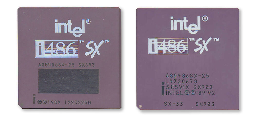
As for all factory-remarks, the addition is quite obvious. Intel probably binned twice these CPUs again at the request of a big customer (IBM?) and added the second rating later. Today’s story about factory-remarks is much more unusual because it concerns standard models.

Am486DX4-100SV8B (remarked 5×86)

After I published this analysis some weeks ago, a reader told me he had a strange Am486DX4-100 that seemed to be a AMD 5×86. After a careful look at the printings that looked 100% genuine at first sight, he was kind enough to lend it to me for further investigation with the UCA. Here it is:
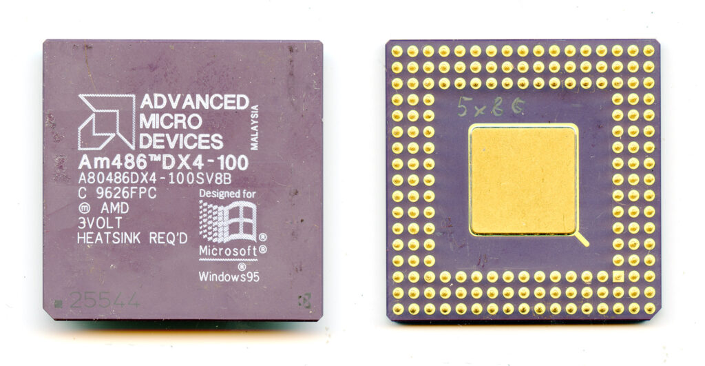
The “9626” date code tells us it was manufactured in late June or early July 1996, which is quite late for a Am486DX4. I immediately noticed the 25544 package code, only used for the 350 nm die. This die was the basis of all Am486DX5 and Am5x86. The “C” stepping was also unusual as the Am5x86 is based on the A-step (from November 1995) or B-Step (from March 1997). A “C” Stepping build in 1996 is incoherent with the 5×86 line, but very coherent with the 486DX4 (later 486DX4 in the latest “C” Stepping were built on the 25498 package in May/June 1996). So it was time for a test on the Universal Chip Analyzer:
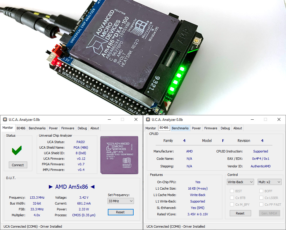
 

WOW! There is no doubt: this CPU is really based on the standard 350 nm die with a fully enabled 16 KB Write-Back L1 cache and a working 4x multiplier. Actually, it can even be overclocked easily to 133 MHz. All specs, including power consumption and CPUID (0x4F4), make it indistinguishable from an AMD 5×86. This CPU can of course also work with a 3x multiplier like an AMD 486DX4-100 (CPUID drops to 0x494).

After some research, it seems that all CPUs based on the 25544/C package are marked as 486DX4-100SV8B while being really DX5 SV16B (5×86). AMD produced them for quite some time between February 1996 and March 1997. They probably stopped the production of the old 500 nm die in early ’96 but still had some demand from customers for DX4s, so they just used the new 350 nm die and marked these CPUs as DX4-100s. As long as you use the default x3 multiplier, they behave exactly like the old one … except for the cache size.

Has Intel also done such weird things? I could have sworn no way. I was wrong…

Intel 486DX2-66 SK080 (remarked DX4)

The same reader also sends me a DX2-66 that could be “really a DX4-100”. That sounded odd and really unlikely to me because Intel has a strict policy on S-Spec. Intel DX4s also have a specific CPUID to help distinguish them from DX2s by software. Unlike AMD 486s, this CPUID does NOT change with the multiplier used, so it’s strange to have a DX2 with a DX4’s CPUID. Here is the original CPU:
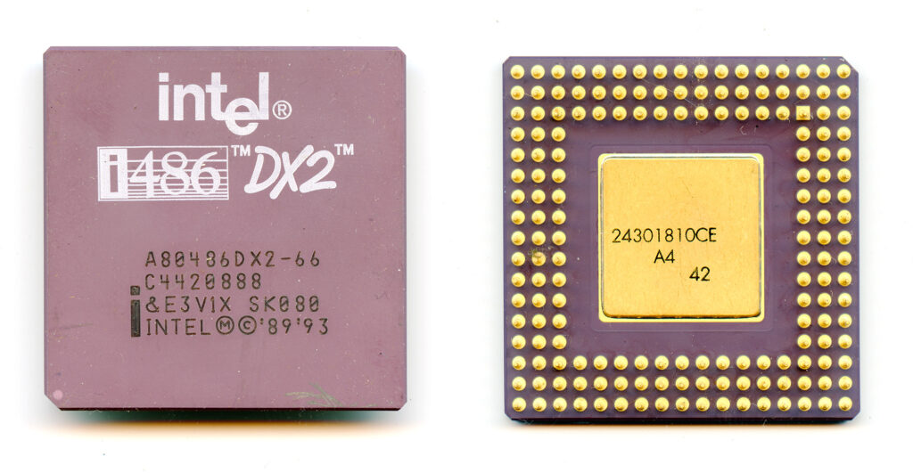
Everything looks genuine here. SK080 is one of the least common S-Spec for Intel DX2s. The only other S-Spec beginning with “SK” is the extremely rare SK058. The SK080 is a 3.3V SL-Enhanced part which seems to have been produced only between WW18’94 (May 1994) and WW48’94 (November 1994). Let’s plug in into the UCA:
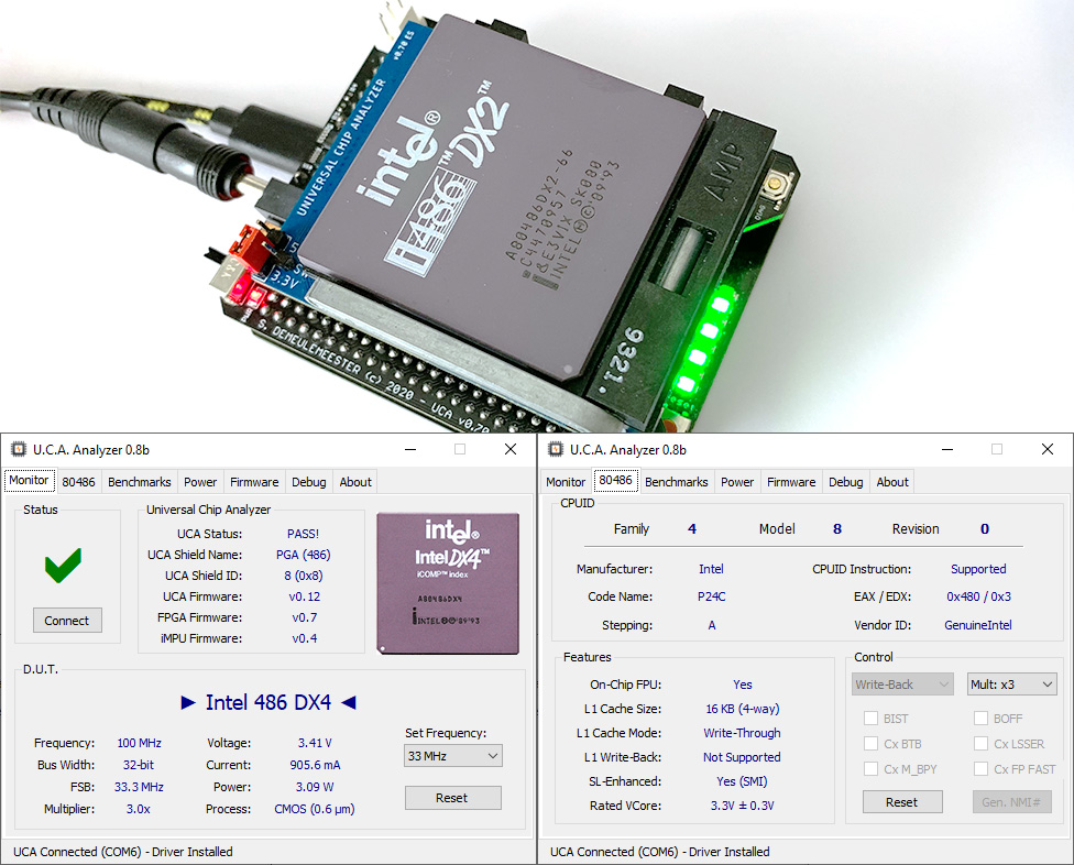
Awesome! This is really a DX4 factory-downgraded to DX2-66. The 0x480 CPUID leaves no doubt about the original die used here. The usual power consumption and the ability to work fine at 3.3V at 100 MHz let me think it’s probably a DX4-100. With the multiplier set at 2x, the SK080 also works at 2×33 MHz as expected for a CPU marked as a DX2-66. To be 100% sure, I was able to find another sample to confirm these findings.
The UCA 386 Adapter now supports AMD & IBM 386s

 IBM 386

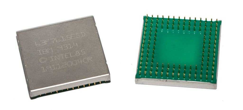
As like all previous microprocessors, Intel licensed the i386 design to third parties. AMD was the only one legally allowed to sell Intel-based 386s to customers (as bare CPUs), but IBM was granted the right to produce some Intel 386s for its own use. They don’t look like a standard ceramic CPUs : IBM used a plastic substrate and a metal cover to protect the die and help with thermal dissipation. Here is how they look like.

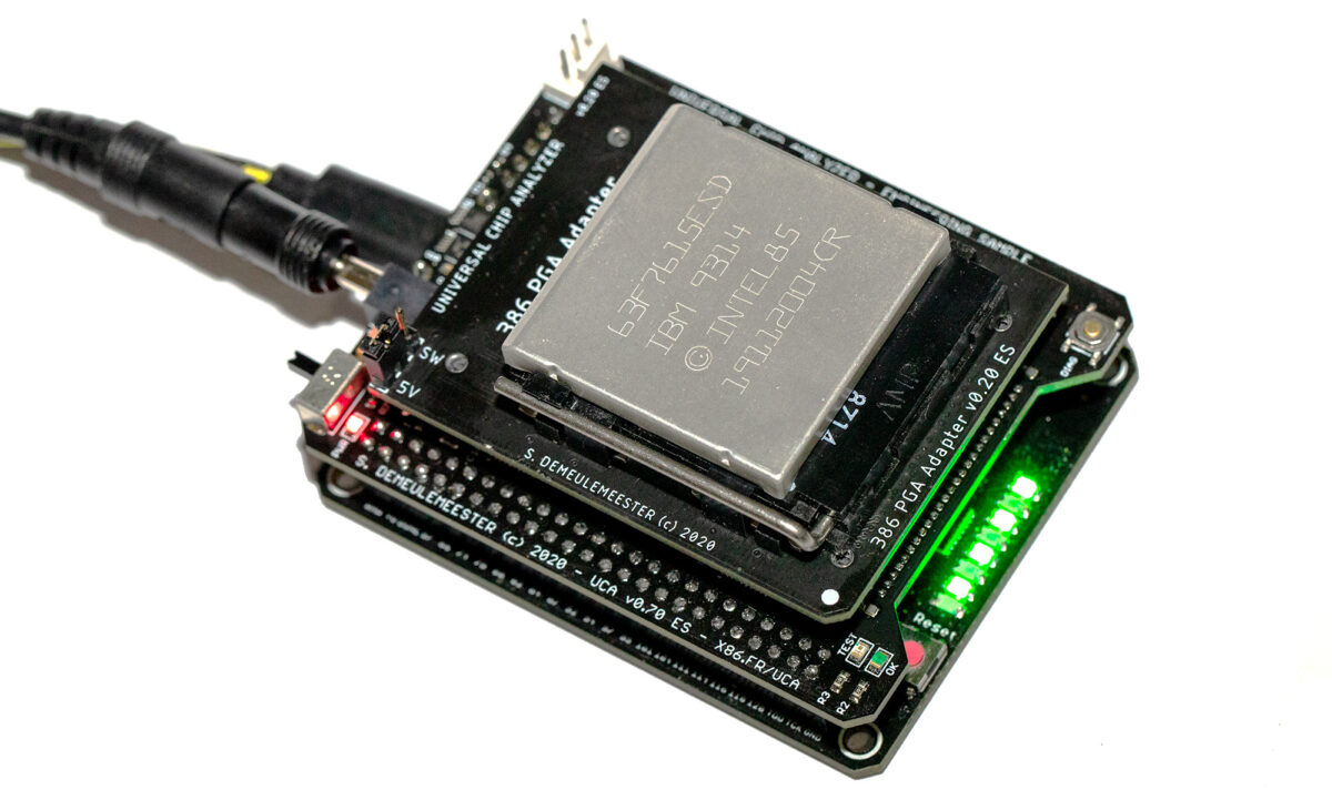
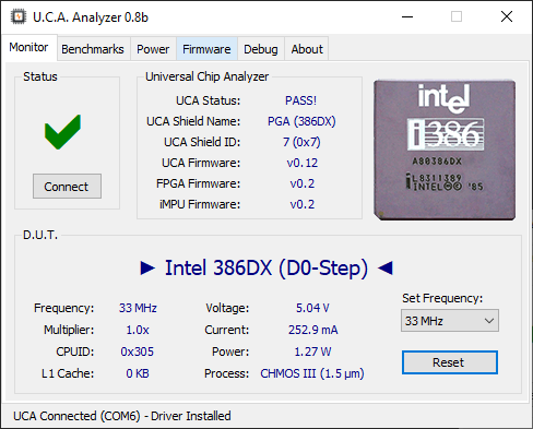
IBM 386If the packaging is different, the internal die is the same as on Intel 386s. 7 different IBM part-numbers are actually known: 23F7189 (?? MHz), 32G6633 (25 MHz), 51F0352 (20 MHz), 51F1783 (20? MHz), 51F1784 (20 MHz), 51F1797 (25 MHz) and 63F7615 (25 MHz).I was able to put my hand on a 51F1784 and the later 63F7615. I tested both on the Universal Chip Analyzer. There is no “Pin 1” mark so I had to guess where is pin 1. Fortunately, the UCA has  strong over-current and short-circuit protection. Let’s start with the 63F7615 :

This one is able to work fine up to 33 MHz, with a CPUID set at 0x305, similar to Intel 386 based on the D0-stepping. I don’t know for sure the real rated frequency, but it’s probably only 25 MHz. The other one (51F1784ESD) is not able to work at 33 MHz and not even at 25 MHz. The actual (early) UCA firmware only has 16/25/33/40 MHz, so I can only confirm that that my 51F1784ESD works at 16 MHz but not at 25 MHz. According to various sources, it’s probably rated at 20 MHz.

AMD Am386

AMD also produced a lot of Am386DX at 20, 25, 33 and 40 MHz. While the microcode is 100% from Intel, the manufacturing process is different and they had lower power consumption (thanks to the 0.8µm process used by AMD instead of Intel’s 1µm CMOS-IV on the latest i386s).

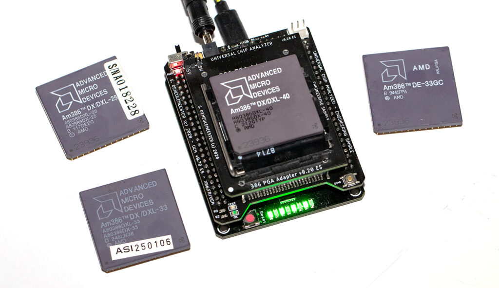
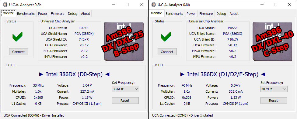
Let’s start with the standard Am386 DX/DXL. I tested one Am386 DX/DXL-25 “B-Step”, one Am386 DX/DXL-33 “D-Step” and another Am386 DX/DXL-40 “C-Step”. All came in the 23936 package from Kyocera.

The UCA tool is not yet able to detect them as AMD, but I’m working on a new algorithm based on power consumption to distinguish them from Intel 386s. The B-Step identifies itself as 0x305, the same CPUID used on Intel’s 386 D0-Step. The DXL-25 was able to work up to 33 MHz. Both C- and D-Step have a CPUID set at 0x308, like the later Intel 386s (D1 step and up).

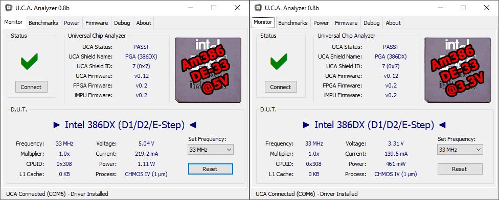
The last CPU to try was the Am386DE-33, an uncommon embedded model. Like the Am386DXL, it uses a fully-static design, meaning it can be clocked down to DC (0 Hz) while retaining all its internal registers content. The biggest difference between the usual Am386DX/DXL and the Am386DE is the disabled Paging Unit in protected mode on the latter. Bit 31 of CR0 (used to enable paging) is reserved on Am386DE. Another difference only available on the Am386DE is the ability to work at its rated frequency with a much lower voltage (down to 3.0V). And it works fine:

At 3.3V, the power needed drops by a huge margin, from 1.1 Watt to as low as 461 mW (0.46W). That’s a -60% power reduction!

[Guide] Am486 Die & Packaging

After weeks spent to test A LOT of AMD 486 with the Universal Chip Analyzer, messing with a gas torch  to decap some of them and speaking with a former AMD engineer that worked on them back in the 90s, I’m happy to publish here all the information I was able to get! Here it is:

The Ultimate AMD 486 Die & Packaging Guide


PS: If you have any more information about AMD 486, please leave a comment. Thanks!

The Universal Chip Analyzer now supports Intel 386 !

Another milestone has been reached. A new iconic CPU family is now supported by the UCA: the Intel 80386, the very first 32-bit x86 microprocessor! The i386 was originally released in 1985 at 12.5 MHz and 16 MHz. It added a 3-stage instruction pipeline and an on-chip MMU (Memory Management Unit) able to address up to 4 GB of RAM. A giant capacity for that time. The original Intel 386 – then renamed 386DX – comes in a PGA132 package and its frequency was later upgraded to 20 MHz, 25 MHz and finally 33 MHz. Later clones from AMD & Cyrix – not yet supported by the UCA – were also released at frequencies up to 40 MHz.

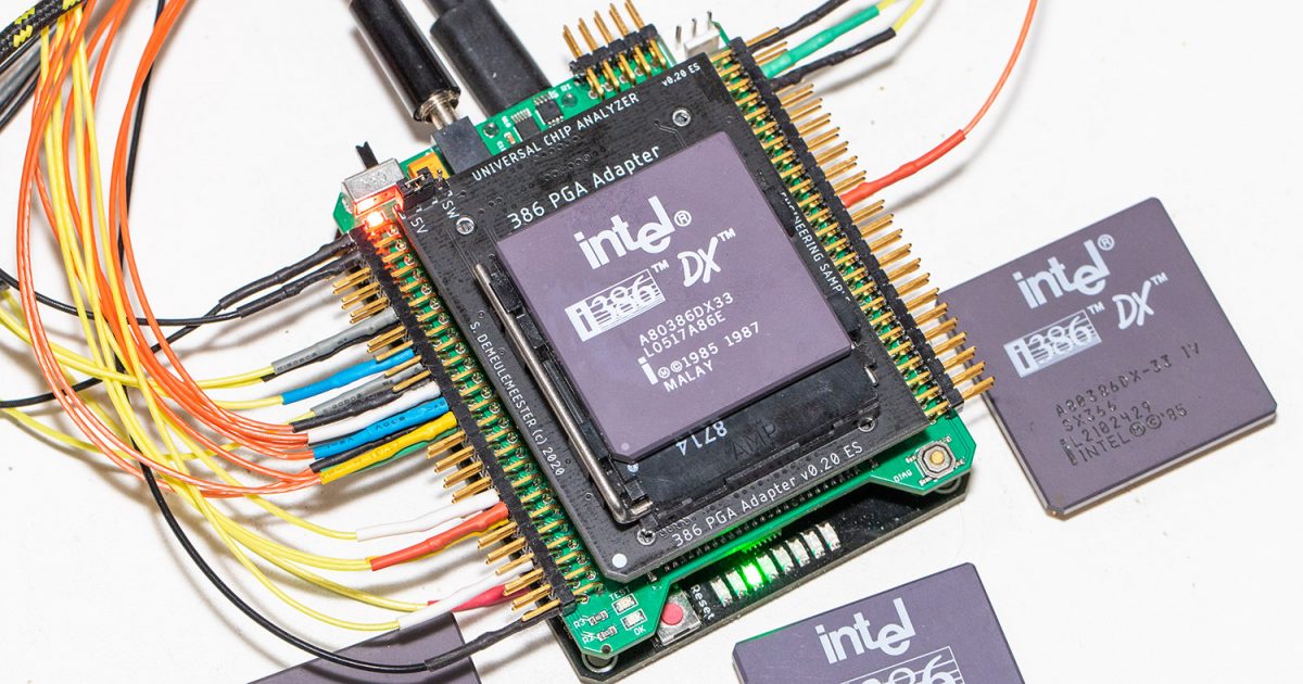
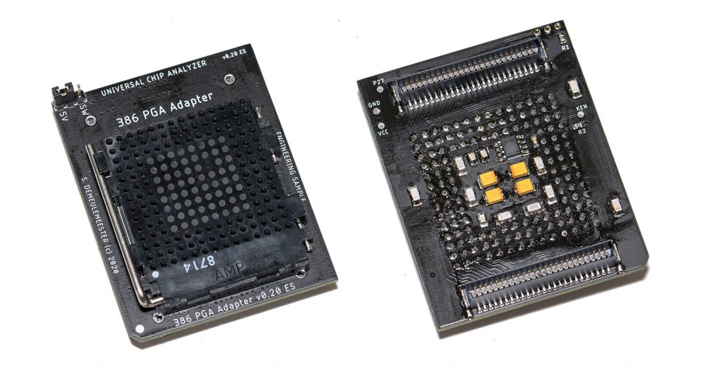
The design of the UCA 386 Adapter was challenging because of the high frequencies involved. While all 486s work with a standard clock input, 386s require a clock-doubled signal with a strong voltage swing (CMOS) between 0 and +5V. Generating frequencies up to 80 MHz (for a 386DX-40) with these requirement was not possible with the UCA architecture, so the UCA 386 Adapter includes an external clock-doubling PLL. For the first try, I used a NB3N511 clock multiplier from On Semiconductor but I was unable to reliably run 386s at more than 20 MHz. The UCA is based on a FPGA and timings are crucial.  With the NB3N511, I was unable to successfully match timings because of the lack of phase synchronization between the input clock generated by the FPGA and the doubled frequency fed to the CPU. So I needed another PLL, with 0-delay between input and output.

After some research, I gave the ICS570A a try and it worked perfectly fine. I was able to sync the internal FPGA logic to the clock-doubled CPU signal up to 40/80 MHz, without having direct access to that signal. Some high-quality ceramic decoupling caps were also mandatory to achieve the highest frequencies. I had a bad surprise while looking at ZIF socket for the 386 Adapter: for some reasons, PGA132 ZIF Socket are extremely expensive and I was unable to source them at a decent price. I bought some at ~$25 each, but if you can help me find more at a lower price, please drop me an email!

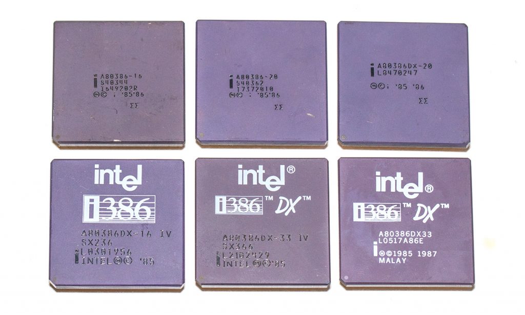
The 4 standard test frequencies for 386 are set to 12.5 MHz, 25 MHz, 33 MHz and 40 MHz. Right now, only Intel 386 are supported, but I’m working on AMD, Cyrix, etc. clones and I’m confident the UCA will support them all very soon. Here are the i386 I have for testing:

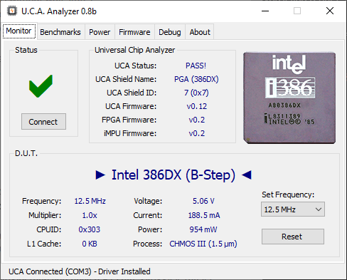
  1. The first one is an early 386 clocked at 16 MHz and produced in 1986. The ΣΣ sign engraved shows that it has been tested free of the infamous 32-bit multiplier bug (more on this on a later post). According to this source, the S40344 S-Spec is a B1 stepping. This is confirmed by the CPUID displayed by the UCA Analyzer tool: 0x303. At 12.5 MHz, this CPU requires about 188 mA at 5V (a bit less than 1W).

  1. The second one is very similar to the first one, except the rated speed at 20 MHz. Still the same B1-Stepping, same CPUID, same ΣΣ, same power consumption, same everything. It also can’t be overclocked at 25 MHz.
    .
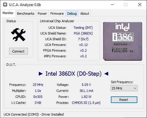
  2. The third one is also rated at 20 MHz but don’t have any S-Spec. It has been assembled in November 1988, more than one year after the previous one. The CPUID is different at 0x305, which indicates a D0 stepping. Surprisingly, the power consumption is 10% higher, at ~212 mA for 5V at 12.5 MHz. Maybe Intel added some logic to solve the numerous erratas in previous stepping, maybe it’s just sample variation. Anyway, the D0 stepping still uses the CHMOS III (1.5 µm) process. This chip can be overclocked at 25 MHz

  1. The fourth one is a 16 MHz marked SX236 and build with the more advanced CHMOS IV process. The CPUID is 0x308, which is used by Intel for D1, D2 and E Stepping. The last stepping is usually marked on the chip, so we can guess it’s a D1 or D2 stepping. Power consumption drops from 212 mA to 147 mA, thanks to the 1 µm process (instead of 1.5 µm). Unfortunately, it can’t work at 25 MHz.
    .
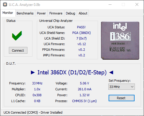
  2. The fifth one is a A80386DX-33 made in 1992 with s-spec SX366. It’s the faster clock speed Intel released for a 386DX. The CPUID is still set at 0x308 but the stepping is clearly more advanced: the power consumption drops to 126 mA while using the same CHMOS IV process than the previous one. This particular CPU requires 126 mA at 12.5 MHz, 206 mA at 25 MHz and up to 261 mA at 33 MHz. It can’t be overclocked to 40 MHz.

  1. The last one is much newer than the others. It was manufactured in 2000 and uses the E-Stepping, as stated by the last letter of the lot code. Aside from this, all specs look identical to the SX366. Measures are also the same and it doesn’t work at 40 MHz.

Stay tuned for more exciting news about the UCA!