

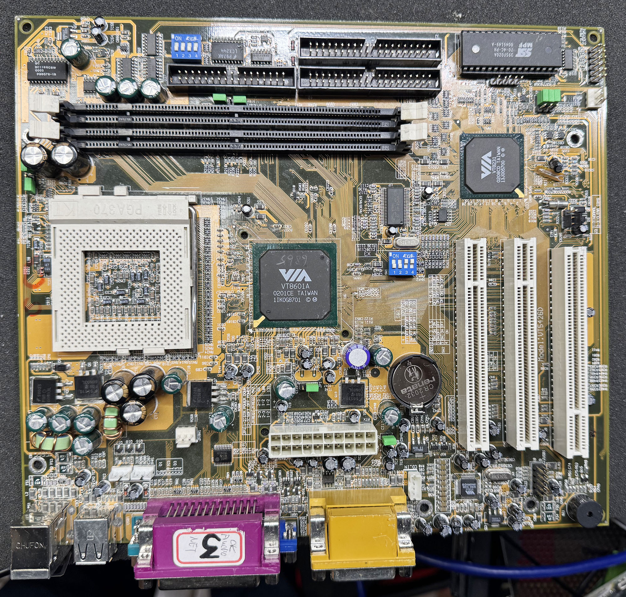
At first sight, the VT5426D board is very similar to the previously analyzed VT5292A. Both are based on the Apollo PLE133 chipset with a VT8601A Northbridge, and large areas of the PCB, especially around the CPU and VRMs, are almost identical. On the newer board, we can also notice the lack of a third SDRAM slot, the missing ISA slot, and the last PCI slot replaced with an ACR slot (physically a reversed PCI slot slightly shifted toward the rear).
The ACR (Advanced Communication Riser) was a short-lived PC expansion-card standard introduced around 2000 as a successor or alternative to AMR and CNR. It was developed by the ACR Special Interest Group, founded by companies including 3Com, AMD, ALi, Conexant, Lucent, Motorola and VIA. It provided a low-cost riser slot for communication and multimedia functions such as software modems, LAN, broadband, wireless networking, and AC’97 audio, while relying on the motherboard chipset for much of the logic. In practice, ACR was mainly used on a limited number of early-2000s motherboards and was quickly phased-out by more integrated onboard functions.
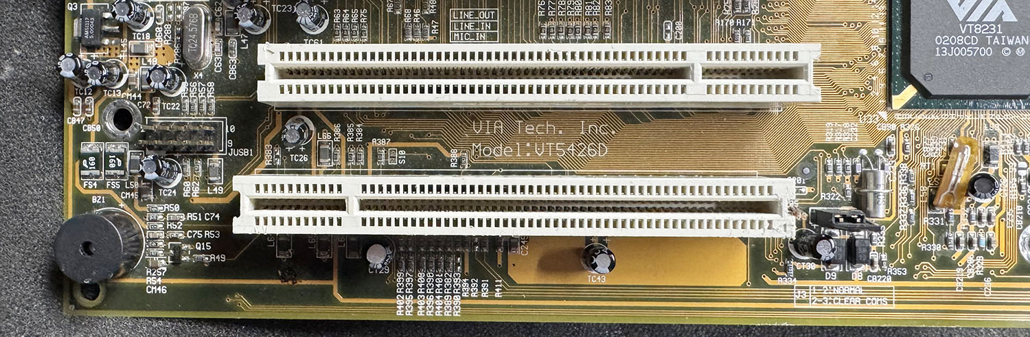
But the main difference is obviously the Southbridge, as the VT5426D is based on the newer VIA VT8231, while the previous VT5292A used the older 686B. The difference between the two is small: basically, the VT8231 is a 686B with an integrated 10/100 Ethernet MAC controller. That’s quite strange, because the VT5426D does not have an onboard PHY to make it usable. My first guess was that this board may have been used specifically to debug an ACR card, which could carry a simple PHY and provide a cheap network interface. But the timeline does not quite match: this VT5426D is a late-2001 board using an early-2002 chipset, while the first ACR 1.0 specification was announced in February 2000, almost two years earlier.
So why the hell did VIA produce a new development motherboard lacking the required PHY and RJ45 connector to test the only new feature of its new Southbridge? Let’s try to boot this board and continue the investigation. Fortunately, as with the previous one, it has very little damage and no bad capacitors (I promise this won’t be the case with all the other boards…). The board booted fine on the first try.
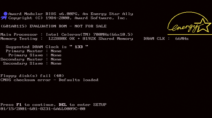
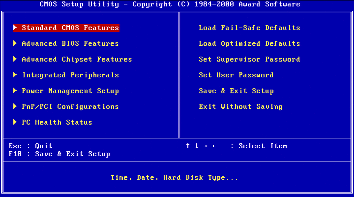
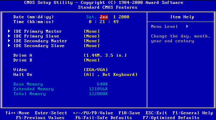
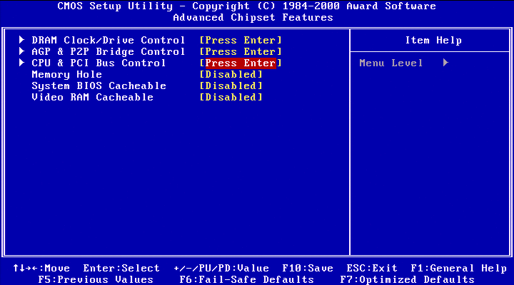
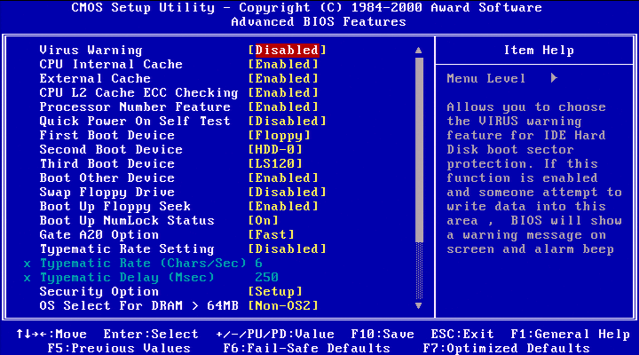
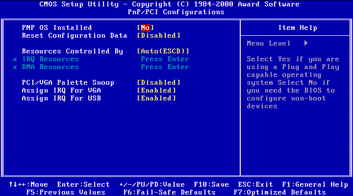
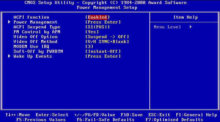
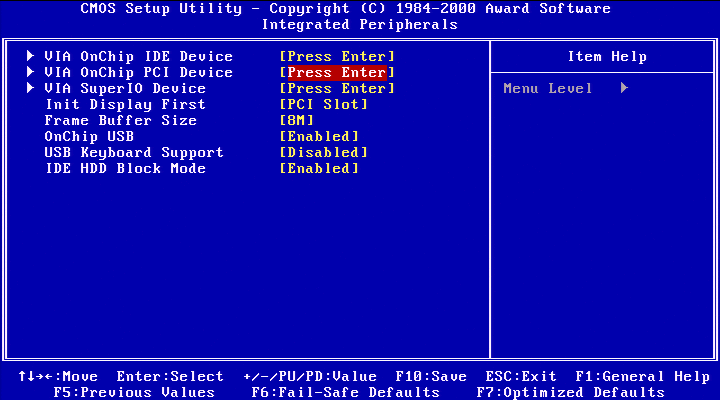
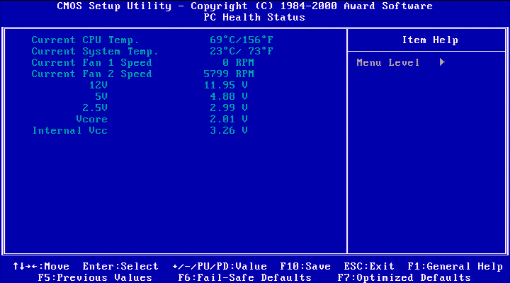
The Award BIOS string identifier for the VT5426D is “01/15/2001-601-8231-6A6LO009C-00”.
The startup string is “(601A0115) EVALUATION ROM – NOT FOR SALE”.
That’s quite interesting. The BIOS is dated January 2001, while the board appears to have been assembled more than a year later: the chipset manufacturing date is late February 2002. This is very unusual, as BIOSes from this era were usually updated quite frequently to support the latest CPUs. The only reason to use such an old BIOS would be for a fixed hardware configuration over a long-term period, for example with the same CPU. Indeed, all mentions of settings dedicated to supporting various CPUs, which were present on the VT5292A, have been removed from the PCB silkscreen.
But the most obvious hint about the true nature of this board is the BIOS identifier: “6A6LO009C”. This exact ID was used by VIA for the very first EPIA board, announced in April 2002. EPIA, for Embedded Platform Innovative Architecture, was VIA’s compact motherboard family for low-power embedded and small-form-factor x86 systems, introduced in the early 2000s as part of the company’s push toward highly integrated “platform” designs. Built around VIA C3/Eden processors and VIA chipsets, EPIA boards combined the CPU, graphics, audio, networking, storage, and legacy I/O on very small Mini-ITX boards (a very compact 17 × 17 cm form factor introduced at the same time and still used today).
It looks like VIA gradually shrank a PLE133 reference board, from MicroATX to the initially proposed “ITX” form factor, and finally to the much more ambitious Mini-ITX form factor, with the following timeline:
-
- January 2001 : VT5426D Development MicroATX form factor (24.4 x 24.4 cm), Socket 370.
- March 2001 : VT6009 Development board in the first proposed ITX form factor (21.5 x 19.1 cm), Socket 370. Note the ACR port. Following the success of this board at CeBit 2002, VIA probably decided to shrink the form factor even more.
- November 2001 : VT6010 Reference board for the final Mini-ITX form factor (17 x 17 cm), Soldered VIA Eden ESP (low voltage VIA C3)
- April 2002 : First commercial Mini-ITX boards under the EPIA line. Soldered C3 (EPIA 800, fan) or Eden (ESP 5000, fangless) CPU.
- January 2001 : VT5426D Development MicroATX form factor (24.4 x 24.4 cm), Socket 370.
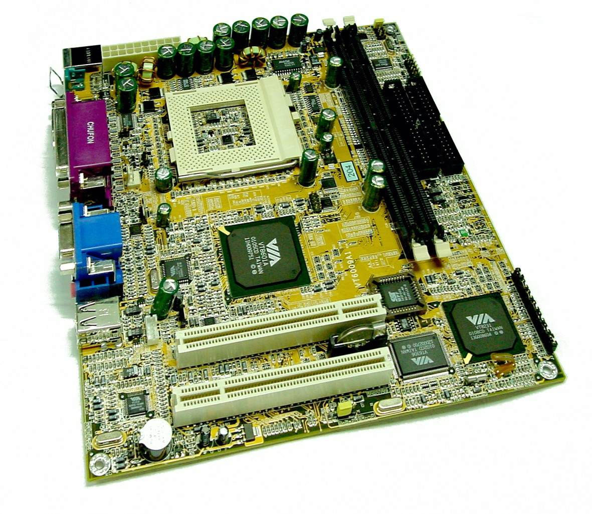
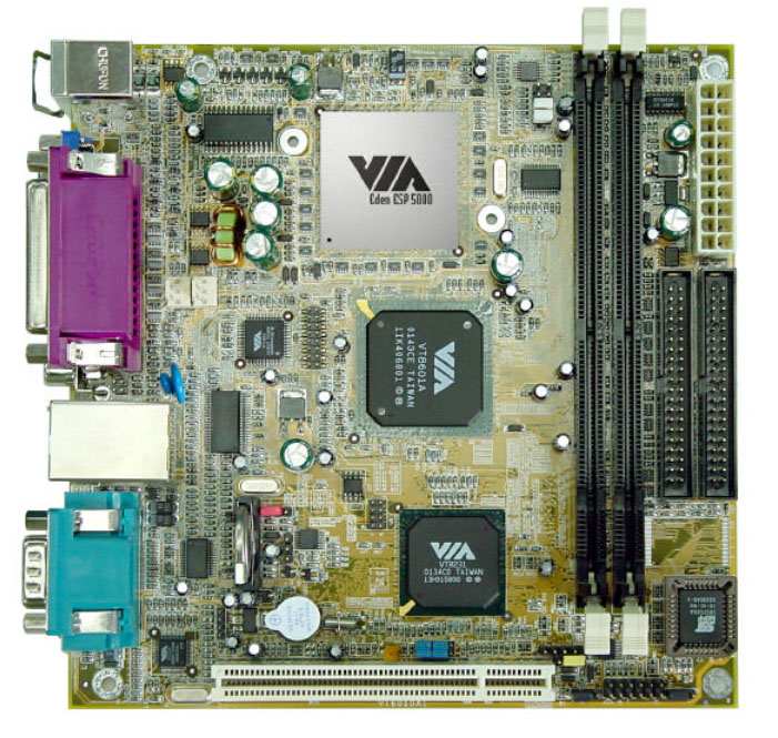
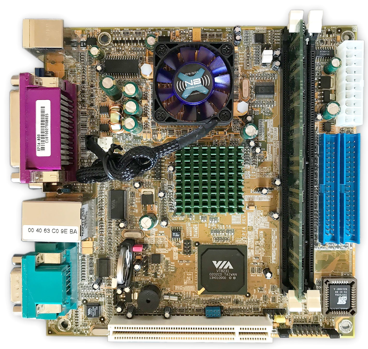
All these boards are based on the Apollo PLE133 chipset with the VT8231 Southbridge and use the same overall schematics, with the same PLL, audio codec, BIOS flash chip, and a similar architecture.
These boards were so similar, and the VT5426D shares so much with the final EPIA board, including its BIOS identifier, that I had a crazy idea: what would happen if I flashed the commercial EPIA BIOS onto the VT5426D? Had VIA removed support for Intel CPUs from the final EPIA BIOS, considering that commercial EPIA boards were only available with soldered VIA CPUs? Or had they kept the code inherited from older development boards, which supported any Socket 370 CPU? Let’s try it.

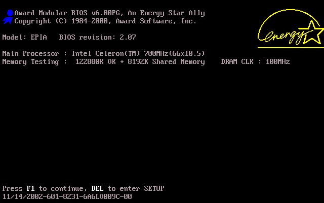
Bingo! The board booted immediately with the EPIA logo and was fully functional, except for the missing network part. It’s quite odd to see a VIA EPIA BIOS running with an Intel Celeron Coppermine CPU. So, in the end, the best guess is that the VT5426D was the missing link that ultimately led to the first EPIA Mini-ITX board.
You can download the original VT5426D BIOS, dated 01/15/2001, here: VT5426D_BIOS