
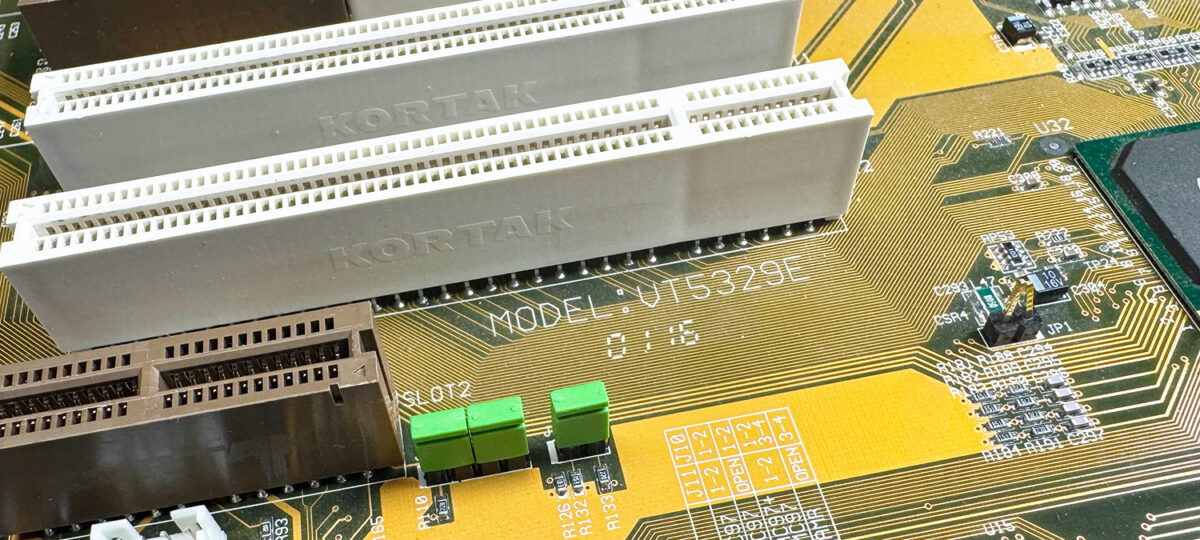
The next board from the cemetery is the VT5329E, a Socket 370 development board which was probably used to validate the switch between Trident to S3 Integrated graphics in early 2000s. Unlike reference boards, which are intended to serve as the basis for commercial motherboards, development boards are primarily designed for R&D purposes. Its unusual form factor leaves little doubt that the VT5329E is one of them.
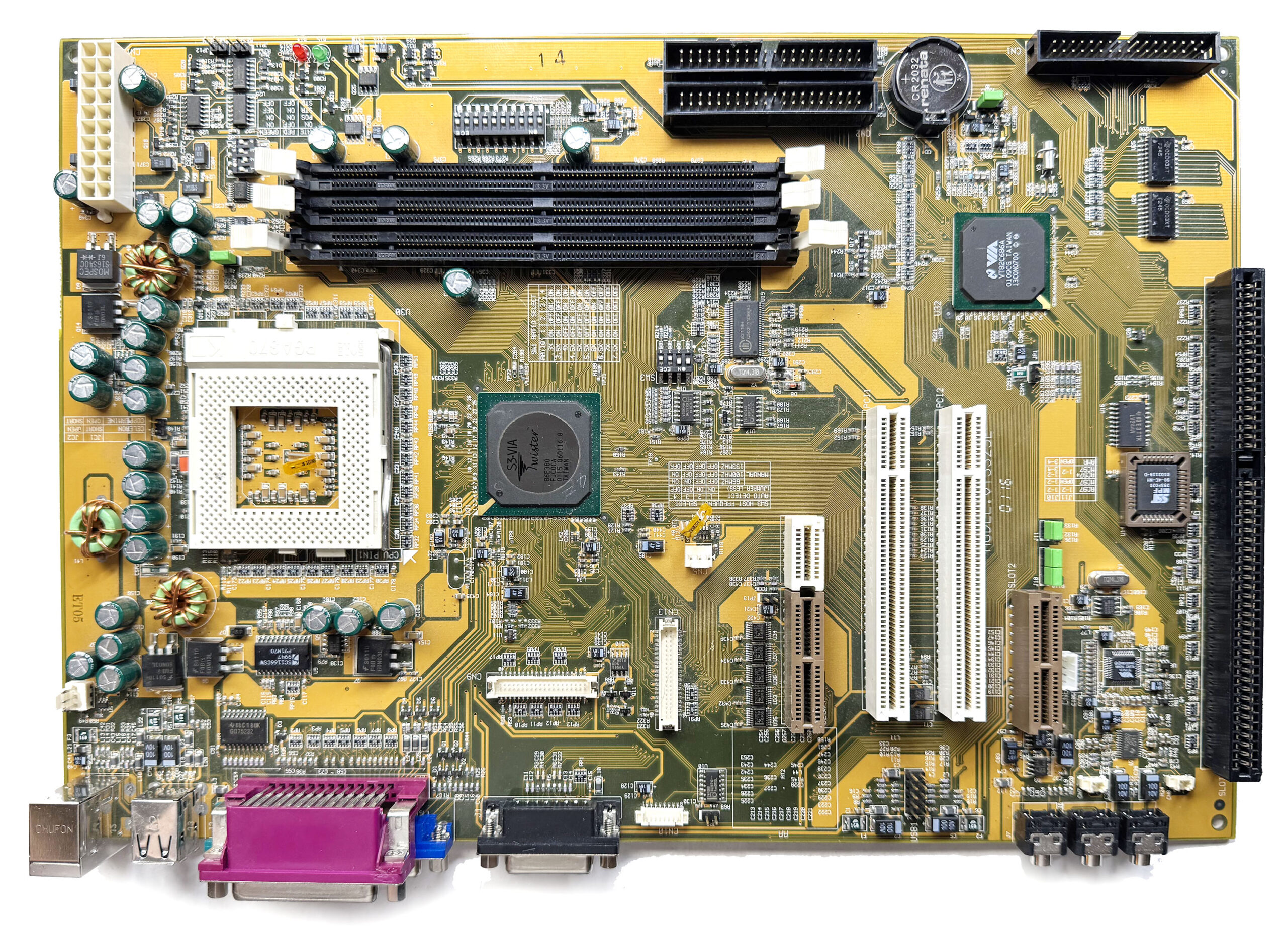 The is significantly larger than a standard motherboard and will not fit in a conventional ATX case. This is confirmed by the unusual placement of the audio jacks, which are aligned with the PCI slots and would prevent the board from being mounted properly. The board has 3x SDRAM, 2x PCI, 1x ISA and 1x AMR slots, and is based on the VT8603 (“Twister”) Northbridge, the first VIA Northbridge to use a S3 integrated chipset instead of the previous Trident IGP.
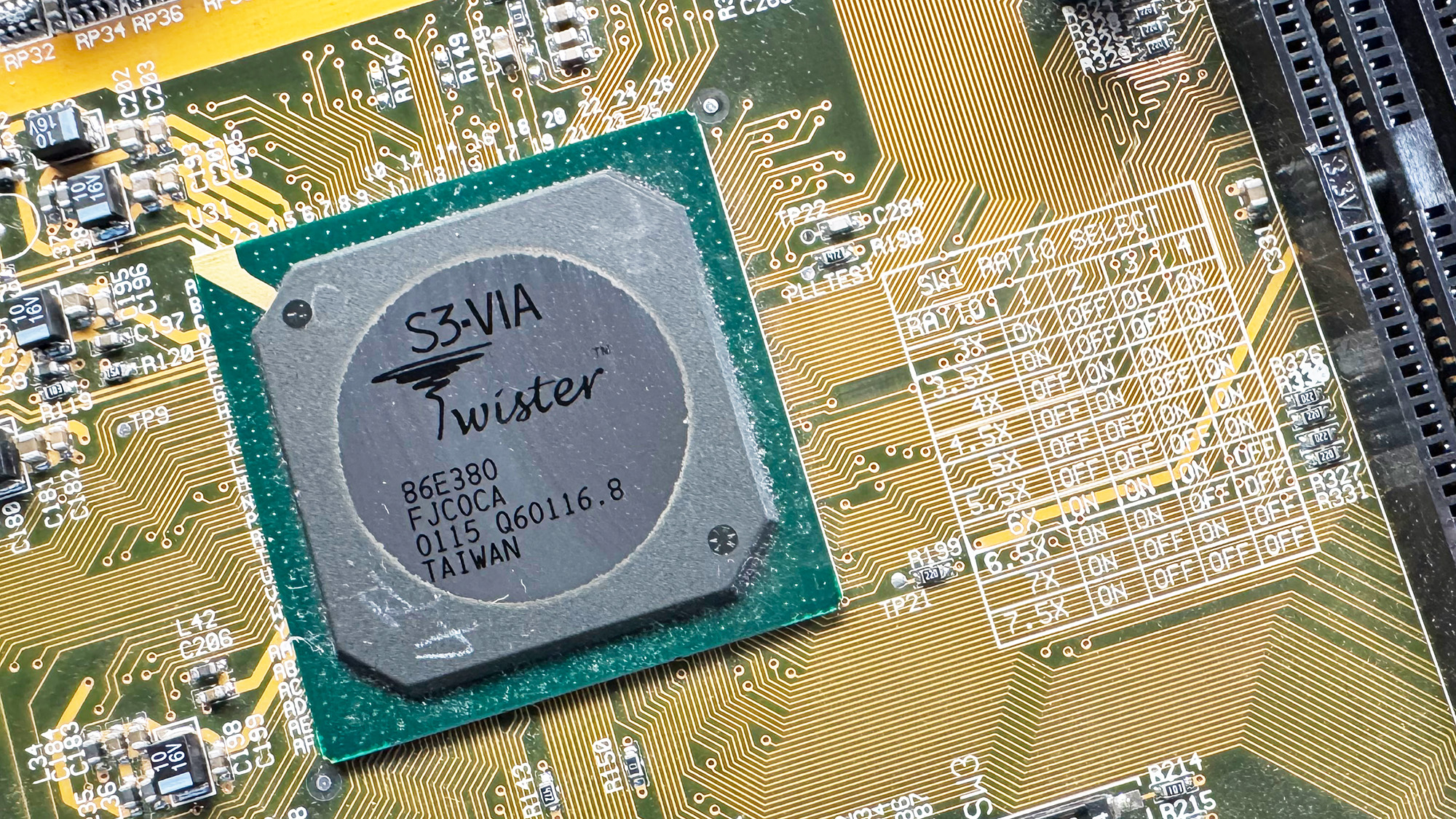 Between 1998 and 2002, VIA’s Socket 370 chipset lineup became rather confusing, with numerous renamings and rebrandings over that five-year period. All VIA Socket 370 IGP northbridges internally use the VIA Apollo Pro 133, or Apollo Pro 133A, northbridge combined with a third-party graphics core. As a reminder, the main difference between the Apollo Pro 133 (VT82C693A) and the later Apollo Pro 133A (VT82C694X) is that the latter adds support for AGP 4X. Both supports FSB 66/100/133 and SDRAM PC133.
Let’s try to summarize everything here.
-
- VT8601 (Apollo PLE133) – The original Socket 370 IGP from VIA. Originally named “Apollo ProMedia”, then “Apollo PM601” and finally “Apollo PLE133”, its final commercial name. Based on the Apollo Pro 133 (not-A), internally connected using AGP 2X to a Trident Blade3D Graphic core. It was officially named “VT8601A” later.
- VT8602 (Apollo PLE133T) – A later revision of the VT8601, based on the Apollo Pro 133A with support for AGP 4X to connect the same Trident Blade 3D Core. This Northbridge is also named “VT8601T” because it supports Intel Tualatin CPUs.
- VT8603 (ProSavage PN133) – Based on the Apollo Pro133A with a S3 Savage4 3D architecture (named “Twister” by S3). This Northbridge has been designed as a Mobile part, with additional features like direct support for LCD panels or more advanced power-saving capabilities. It doesn’t support an external AGP slot. That’s the Northbridge on the VT5329E Development board. VIA used the contraction between “Apollo Pro” and “Savage4” to finally name it “ProSavage”.
- VT8604 (ProSavage PL133/T) – A stripped-down version of the VT8603, with Mobile-specific features removed and still no support for an external AGP slot (IGP is the only option for graphics). It was designed as a cheaper option for the Value Desktop segment.
- VT8605 (ProSavage PM133) – This part is a “high-end” Desktop part with IGP, almost identical to the previous one, but with support for an external AGP 4X slot. Basically, an Apollo Pro 133A with a embedded electrical switch between the internal S3 IGP and an external AGP 4X slot.
- VT8606 (ProSavage PN133T) – A minor revision of the VT8603 with support for Intel Tualatin (CPUs). This Norhtbridge is quite rare and has been used exclusively in embedded computers, SFFs (like early Shuttle barebone) and some elusive laptops. It has been produced up to the early 2010s.
- VT8601 (Apollo PLE133) – The original Socket 370 IGP from VIA. Originally named “Apollo ProMedia”, then “Apollo PM601” and finally “Apollo PLE133”, its final commercial name. Based on the Apollo Pro 133 (not-A), internally connected using AGP 2X to a Trident Blade3D Graphic core. It was officially named “VT8601A” later.
All these Northbridge are usually accompanied by the VIA 686A or 686B Southbridge. As an early board, we have a VT82C686A on the VT5329E:
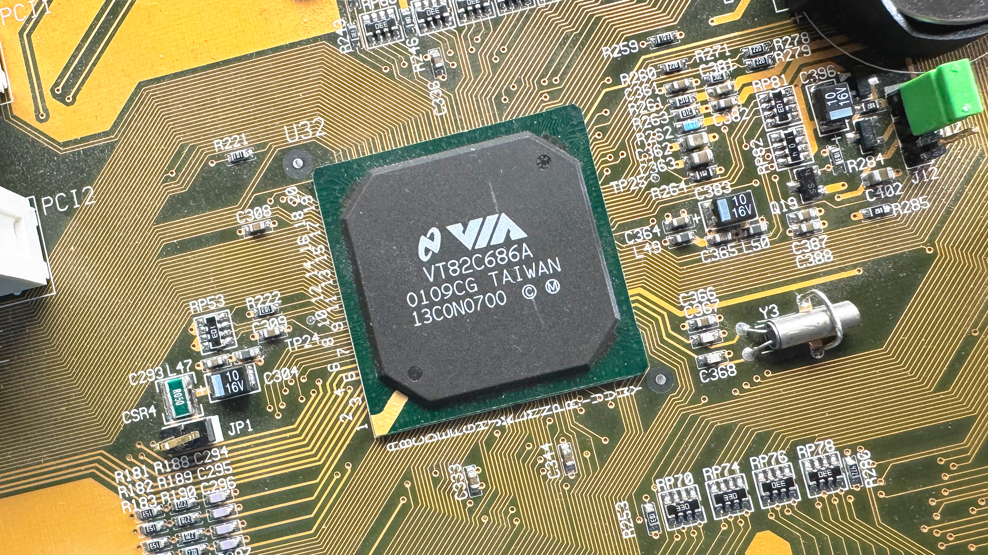 There are not many differences between the 686A and 686B. The latter basically just adds ATA100 (UDMA 5) support. Both supports PCI-to-ISA bridge, AC’97 audio, an integrated Super I/O chip with monitoring, SMBUS and USB 1.1 (up to 4x ports). On the VT5329E, it seems clear that the audio codec part was specifically targeted for evaluation.
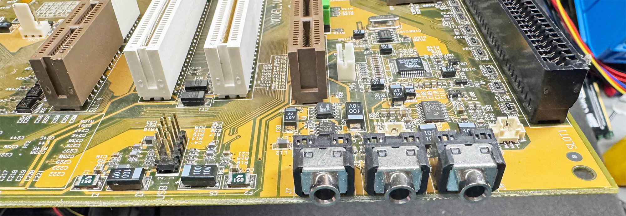 The board has jumpers for AC’97 (provided by a VT1611A), MC’97 (modem counterpart), AC’97+MC’97 and for the dedicated audio/modem codec slot (AMR). Note that this is the older (circa 1998) AMR specification and not the newer CNR standard that was introduced by Intel in 2000.A very interesting point is the strange slot located close to the Northbridge
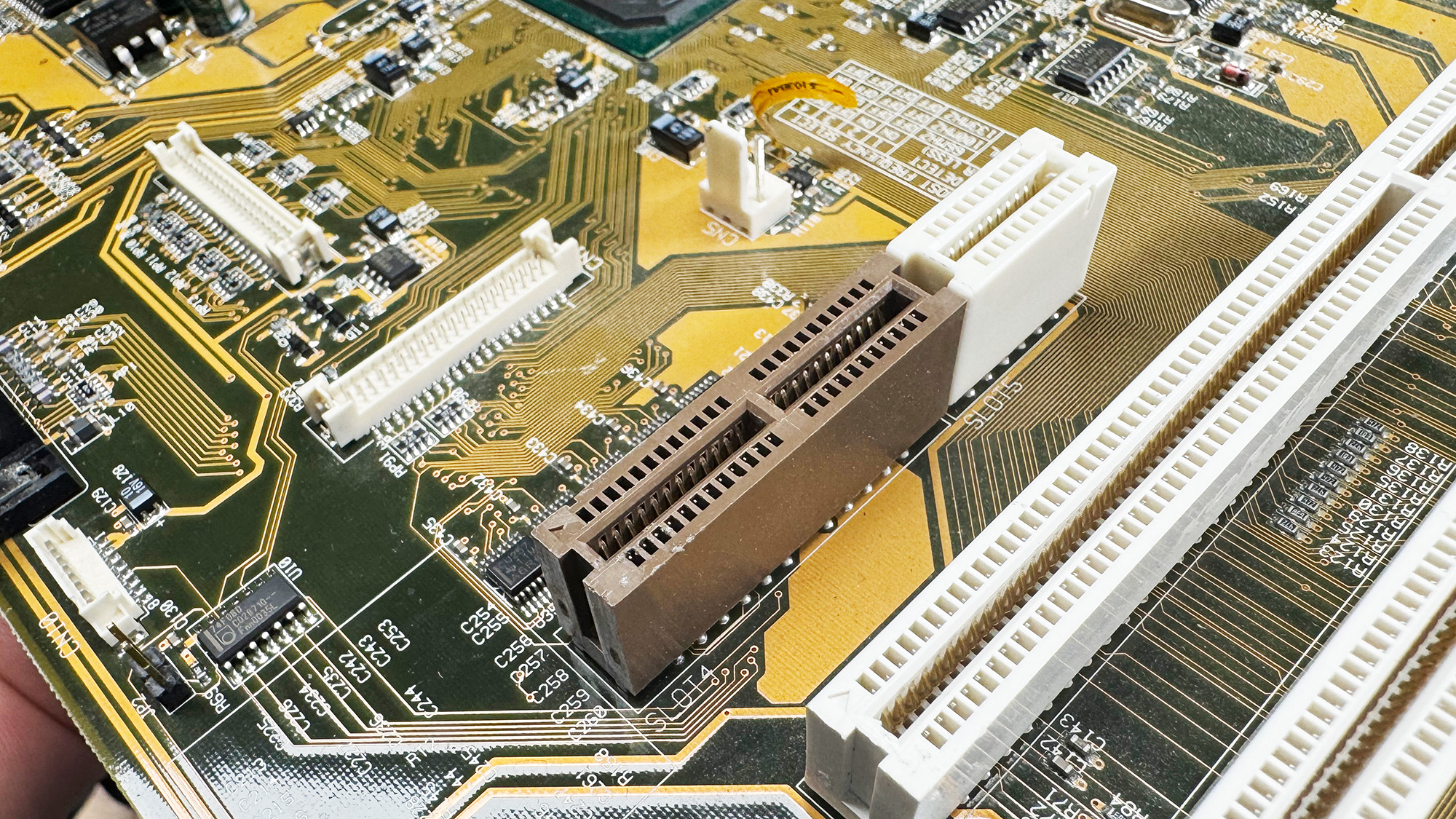 Physically, it resembles an AMR slot with a small white extension similar to the end of a PCI slot. Electrically, however, it has nothing to do with AMR. Based on the PCB traces and the voltage translators located nearby, my best guess is that this slot breaks out the LCD panel signals for debugging purposes.
The VGA port on the VT5329E doesn’t work as expected. It outputs a strangely formatted signal resulting to a scrambled display. It may try to output a LCD panel signal.
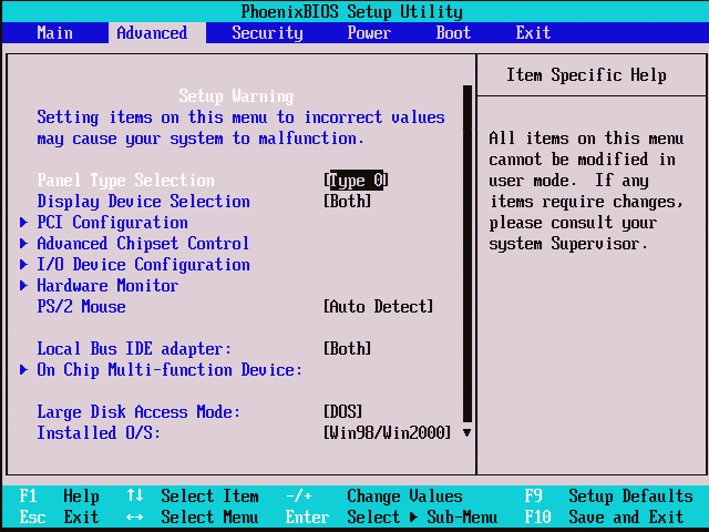
EDIT [2026-08-09] : It does indeed output a LCD signal. To bring it back to standard VGA, flipping the “Display Device Selection” option from “Both” (default) to “Auto” is required. Thank to
With an external PCI card, everything is OK:
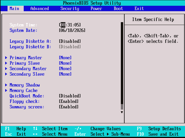
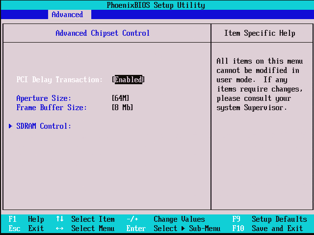
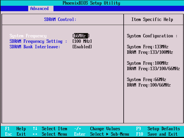
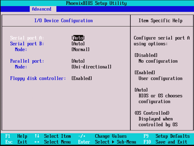
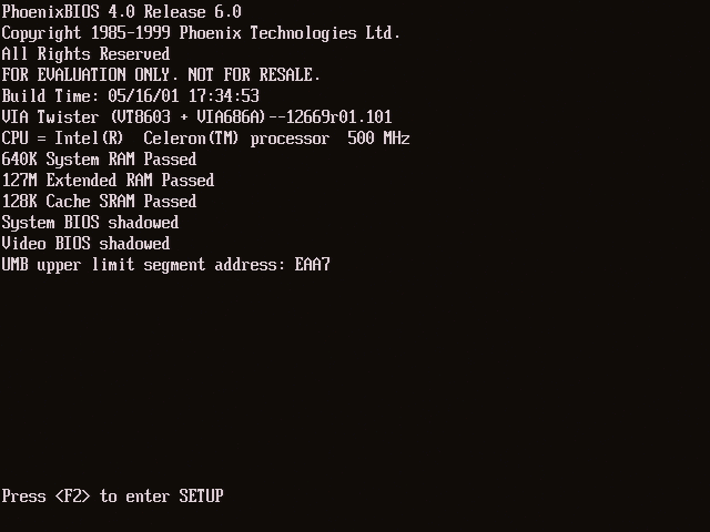 We are greeted by a Phoenix BIOS 4.0 instead of the usual Award 6.00 BIOS. Not really surprising for a Mobile development platform (Phoenix BIOS were much more common in laptop). The boot strings include “FOR EVALUATION ONLY. NOT FOR RESALE” and “VIA Twister (VT8603 + VIA686A) –12669r01.101” with a build date on 2001-05-16. The configuration menu is quite nice:
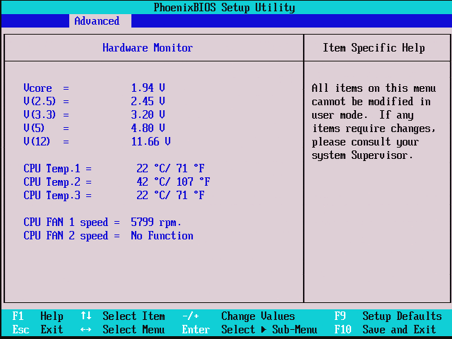
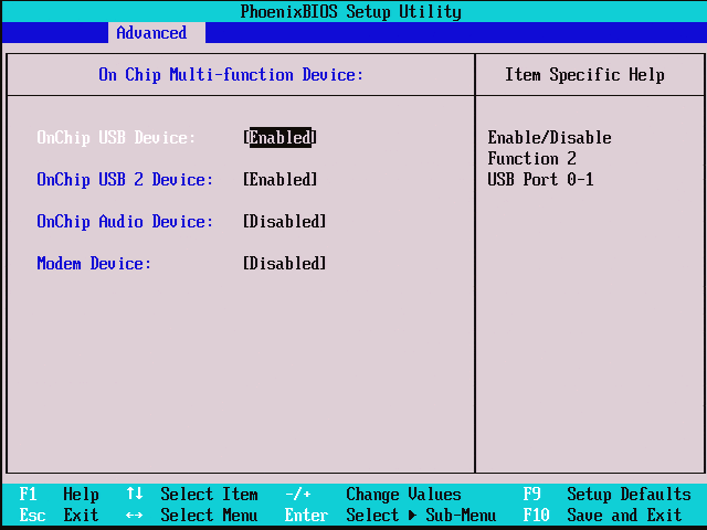
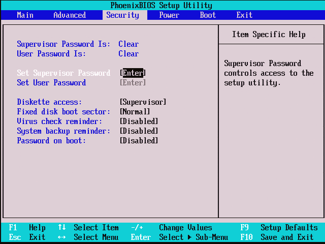
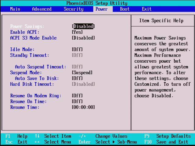
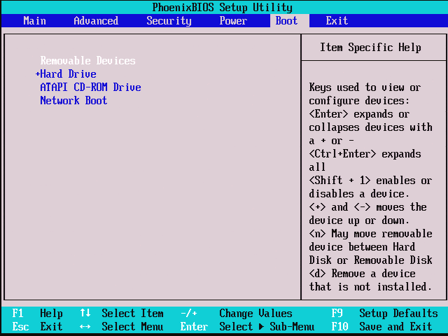
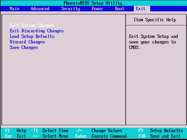
I would have liked to find other system based on VT8603 “Twister” or PN133 chipset, but I couldn’t find a single one. If you have any information about a computer using this Northbridge, just let me know in the comments, I’ll add it here!
The Axiomtek SBC82621 half-size single-board PC uses the VT8606. I’ve got two of them that I picked up on eBay years ago when I started experimenting with single-board x86 computers. Both units came with a power supply that was intended to be hooked into a vehicle’s electrical system, and I’m pretty sure they originally came out of fire trucks, because there was a sub-board under the power supply that said it was meant for fire vehicle control and the boards had soot on them from exposure to diesel fuel exhaust.
They both work quite well. One has the P-III-800 that was installed in it originally, but the other one has a P-III-1200 Tualatin that I swapped into it. Windows 98 installs pretty solidly on it, and if you play your cards right XP works pretty well, too.
You mentioned that the VGA out puts out an odd-looking signal. You’re correct that it’s putting out a signal formatted for an LCD screen, and there’s an LVDS port at either CN9 or CN13 on the board you’re showing above. When it’s set to use both a CRT and the LCD for display, it just stretches the LCD’s display format to fit CRT geometry. The BIOS should have options to set which thing it formats things for by default. It looks like the second screen you show has that option. The “Display Device Selection” option should select between CRT, LCD panel, or both.
Very interesting! I just tested this and indeed, you’re right. The “Display Device Selection” option has two settings: “Both” (default) and “Auto”. Flipping it to “Auto” restore the VGA signal on the VGA port and everything looks fine. I edited the article accordingly.
This might be helpful, as well. There is a copy of the datasheet for the VT8606 available on TheRetroWeb. It’s a preliminary one, but it’s definitely a leg up.
Here’s the link to the TRW page. The link to the datasheet’s about halfway down the page.
https://theretroweb.com/chips/3128
On another note, I’d love to ask about the Universal Chip Analyzer, specifically about being able to build/obtain one myself. I presume that you can see the email address attached to the comment, so if you’re looking to keep the device relatively wrapped up “until it’s ready,” so to speak, I’d welcome an email directly from you to ask about specifics.