With the development of the PGA Shields (now able to support all Intel CPUs from 80186 to 80486) and the rise of demand from collectors, it was time to think about producing a batch of the Universal Chip Analyzer. In January, I finally decided to rebuild everything from scratch to get rid of old issues and restart from a “clean” foundation. The original Mojo v3 board I used since the very beginning was a fantastic tool, but after way too many patches, I encountered “hard” limitations which would have become major issues later. As I don’t want to rework the base FPGA board nor the main interface (IF) board for years to come, the solution was to build the perfect PCBs one time for all.
So, let me introduce the Universal Chip Analyzer v2!
UCA FPGA Base Board
The Mojo V3 was a great tool, but it’s a 2013 Kickstarter product tailored as a development board. I hesitated for a long time to replace the Xilinx Spartran-6 FPGA with a “new-gen” Spartran-7 or even an Artix-7. I finally decided to stay with the Spartran-6 for many reasons.
-
- Xilinx 7-Series FPGA are only available in BGA and not in QFP packaging. That mean more complex PCB and higher manufacturing cost.
- While 6-series are happy with two simple 3.3V and 1.2V linear regulators, 7-series FPGAs requires 3.3V/1.8V/1.35V and 1.0V. That mean noisy DC-DC buck converters, more filtering, and ultimately MUCH higher BOM and assembly costs.
- The speed and logic cells count on the Spartran-6 XC6SLX9-2 are enough for all actual and future uses I can think of. I could have used more Block RAM, but it’s not a limitation.
- Xilinx announced that that this FPGA is a “long term product” that will be manufactured at least until 2027. It’s also quite cheap now (< $10).
Switching to a Spartran-7 or Artix-7 would have just significantly increased the price and overall complexity without adding any feature. The only interesting point I will miss is related to the development toolchain. I could have finally got rid of the infamous Xilinx ISE for the new Xilinx Vivado Design Suite. But after all, I’m now quite comfortable with all the damn ISE’s bugs, so…
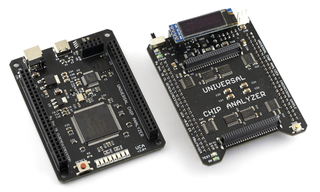
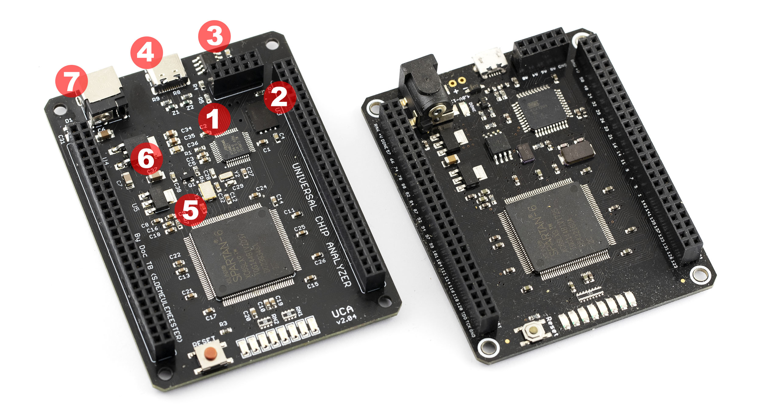
Here is the new Universal Chip Analyzer board next to the old one.
 I kept the overall form factor, just a bit (6 mm) higher, but many components changed.
-
- ARM Main microcontroller – The original 8-bit ATMEGA32U4 (at 16 MHz, with 32 KB Flash & 2.5 KB SRAM) has been replaced with a 32-bit ARM-based ATSAMD21G18. The new MCU is clocked at 48 MHz, Flash capacity is 8x higher (256 KB) and SRAM is now upgraded to 32 KB. It’s also MUCH faster and I have room for many future improvements. While the ATMEGA32U4 was 80% full, the new ATSAMD21G18 is under 20% after a full code rewrite, and with more features added!
- 512 Mb Flash Memory – The original Mojo v3 used a 4 Mb SPI Flash able to store a single FPGA configuration file. With the first UCA, I upgraded the flash to 128 Mb to store up to 40 different configuration bit-files. The final UCA now use a 512 Mb Flash to store more than 150 configurations file simultaneously.
- EEPROM – A small 64 Kb I2C EEPROM to store calibration constants, configuration, serial numbers, etc. has been added.
- USB-C Connector – The good old Micro-USB connector tend to become obsolete. The new reversible USB-C connector will soon become the standard. It is also more robust.
- Better XO. The main 50 MHz oscillator has been upgraded to a 20 ppm, low power one for lower jitter and better stability at high frequency.
- Stronger power filtering – The filtering/decoupling stage was limited on previous board. It is now much stronger, allowing higher noise immunity and better switching speed for fast CPU like 486s. Thermal dissipation has also been vastly improved.
- Power Connector – First prototype of the old UCA v2 used a tiny 1.35mm jack located on the IF board. The final one come with a standard 2.1mm jack with polarity reverse protection. An additional 9V or 12V power supply is mandatory for all supported Ics. I tested some USB to 9V/12V adapter, and they work fine, making testing from a power bank on the field possible.
There are also many layout changes, allowing for example I2C communication from the MCU to IF to Adapter boards.
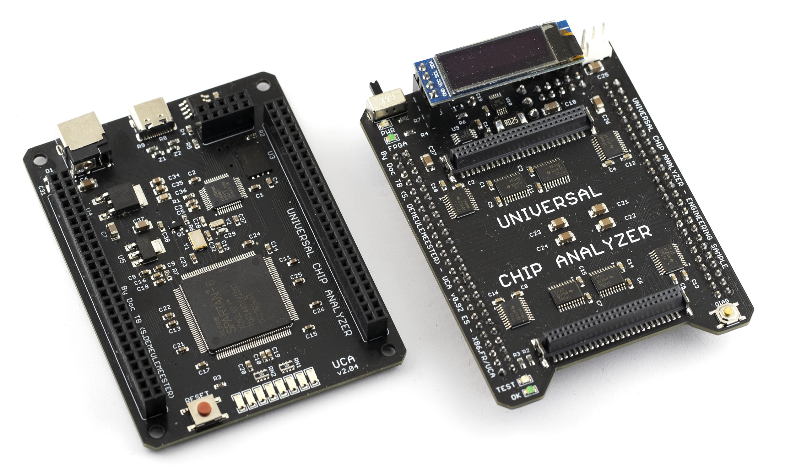
UCA Interface (IF) Board
 The final IF board has been upgraded to perfectly fit on top of the FPGA board. The PCB has been enhanced for reliability while lowering BOM cost. All but one tantalum capacitors have been replaced by MLCC (ceramic) caps. Layout has also been improved for better decoupling efficiency. Along the main voltage transceivers, the UCA IF board includes a 2A DC-DC voltage converter, precision voltage and current monitoring, and adjustable fast overcurrent protection. Voltage can be set by software (25 mV steps). A standard 3-pin fan header is available for high-power CPU like DX4s.

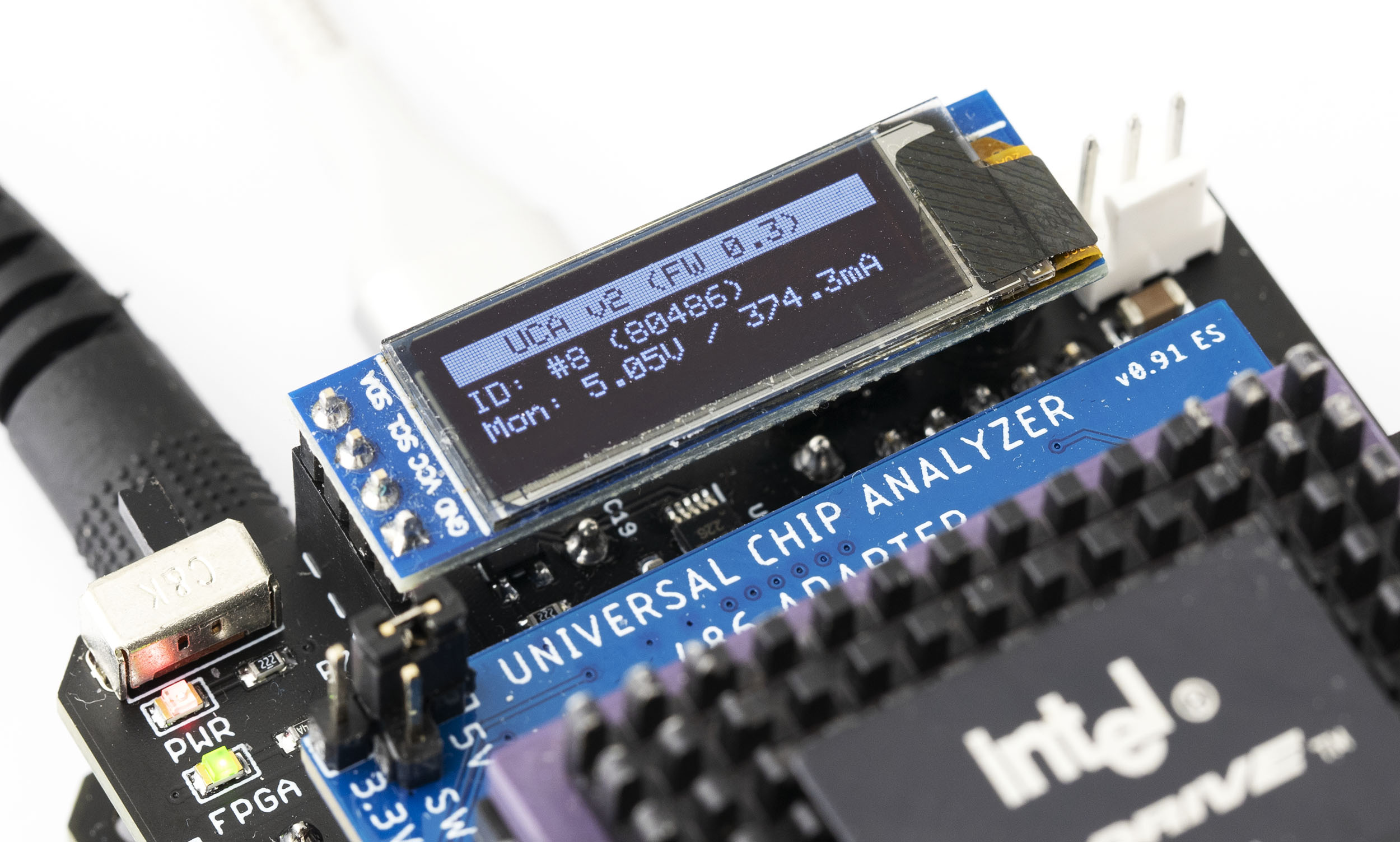
The slightly bigger PCB height allowed an optional 0.91″ 128×64 OLED display to fit on top of the board. It will be used later to display additional information about the test status. Right now, it shows the selected CPU Family and the voltage/current used.
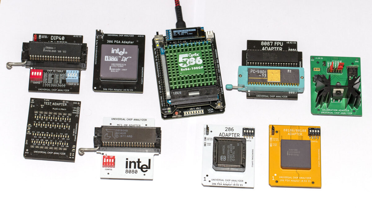
UCA Adapters
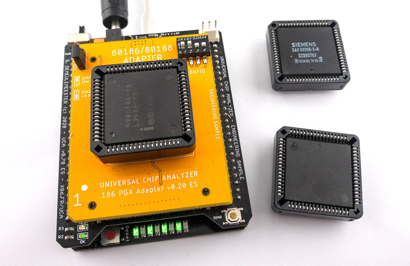
The pinout on both 50-pin connectors located on the IF Board as slightly changed to accommodate previous modifications. I added some new signals to avoid future limitations. For example, the I2C is not passed from the ARM MCU to the adapter boards. Adapter’s ID also changed for their final values, so all currently designed adapters required a small layout change.
Let’s see the currently designed adapter and their current status.
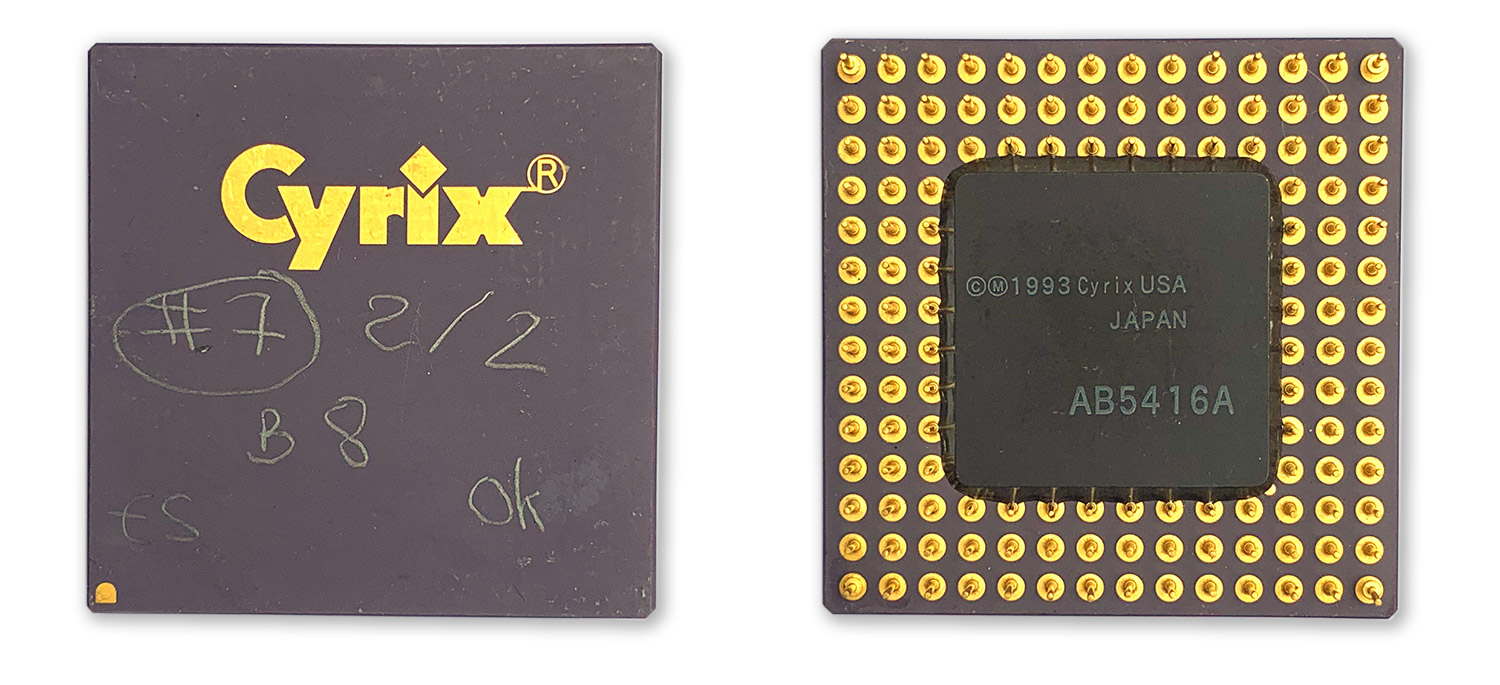
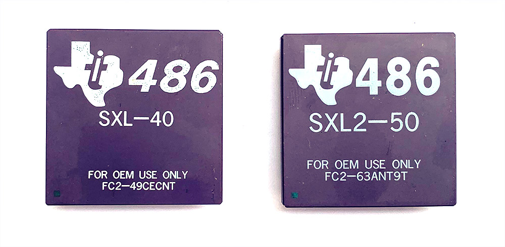
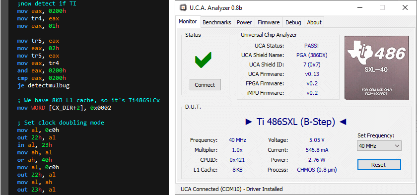
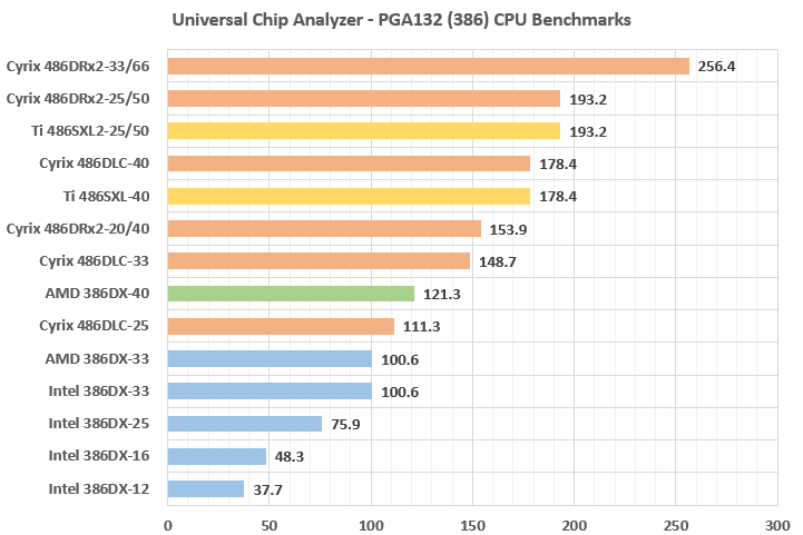
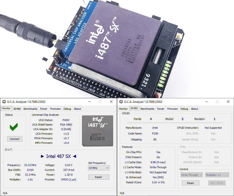
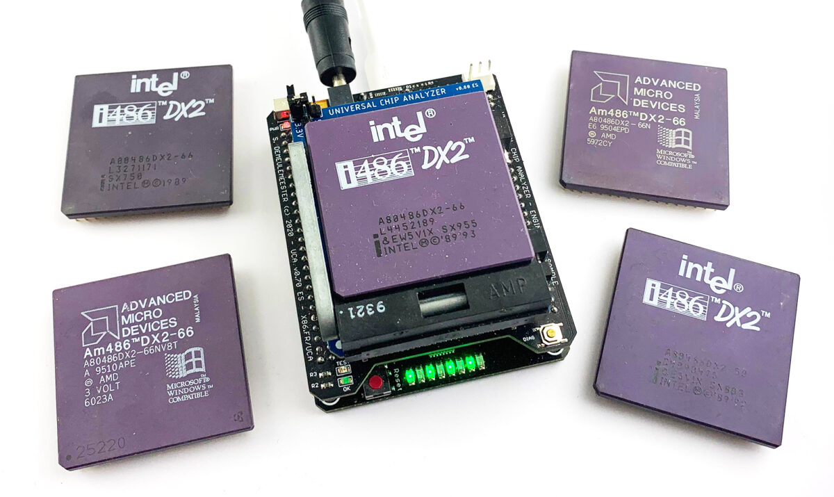
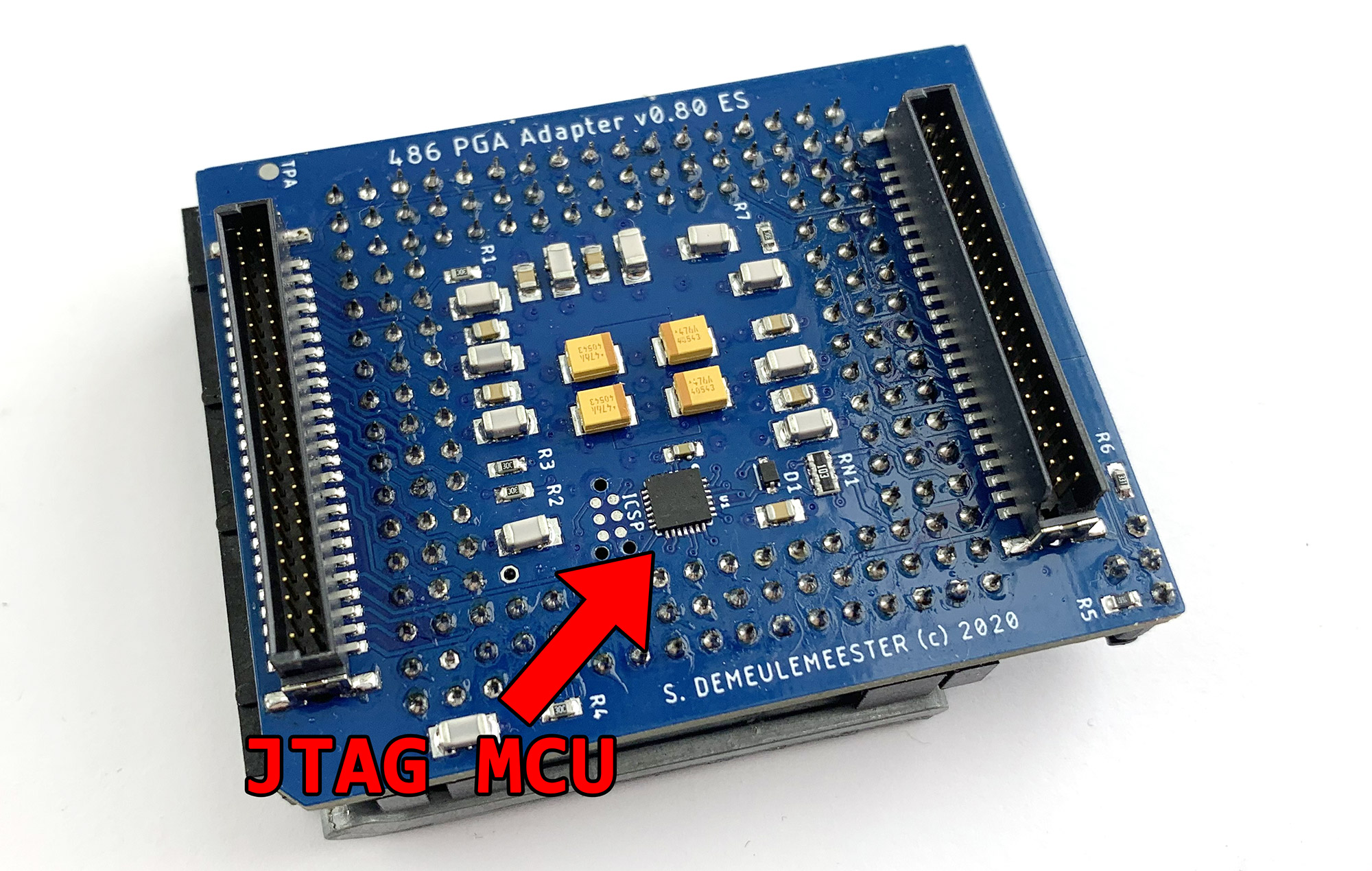
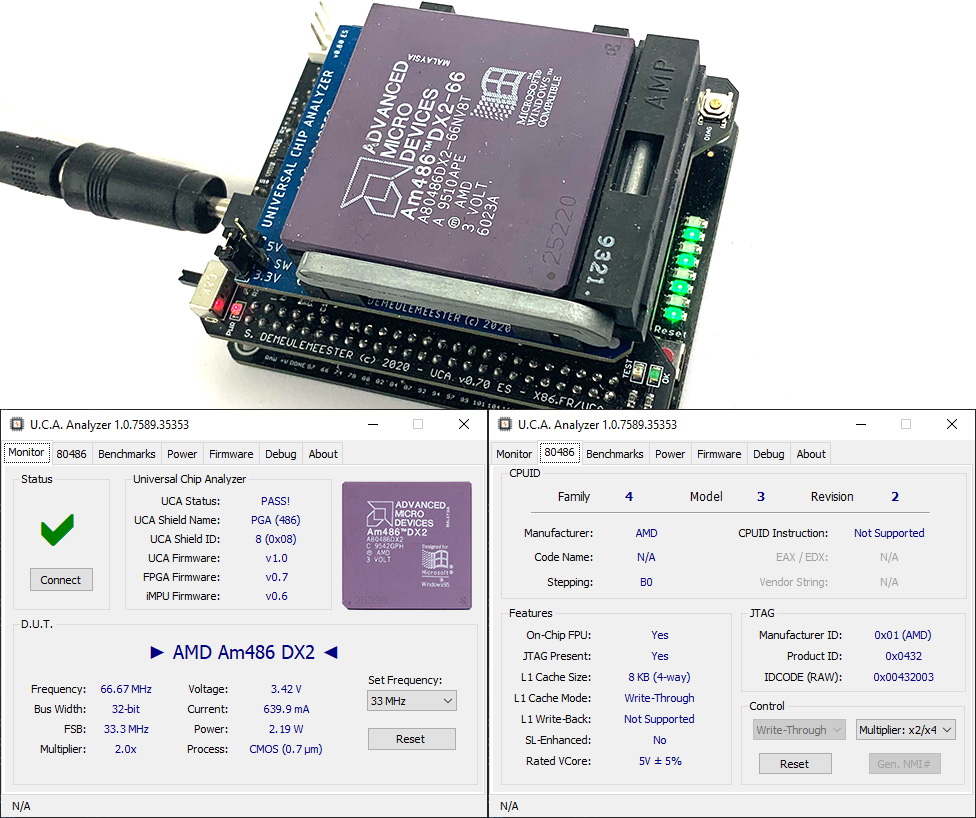
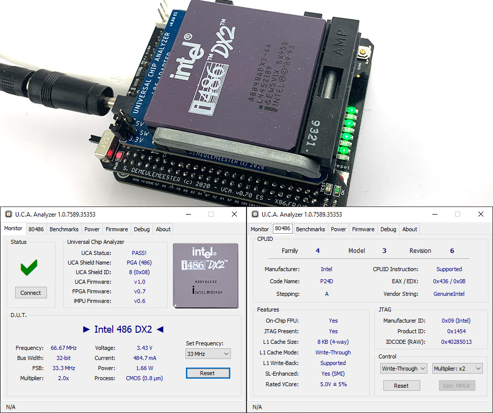
 The 486 adapter has been recently upgraded to support JTAG reading. From a hardware point of view, the adapter is almost finished. There is still a small side feature I would like to add, but it’s a minor modification. The 486 adapter is able to test all 486 ever released, from the Intel 486 SX-16 to the Cyrix 5×86-P133, but also 487s, AMD 586, Ti, UMC and IBM 486s.
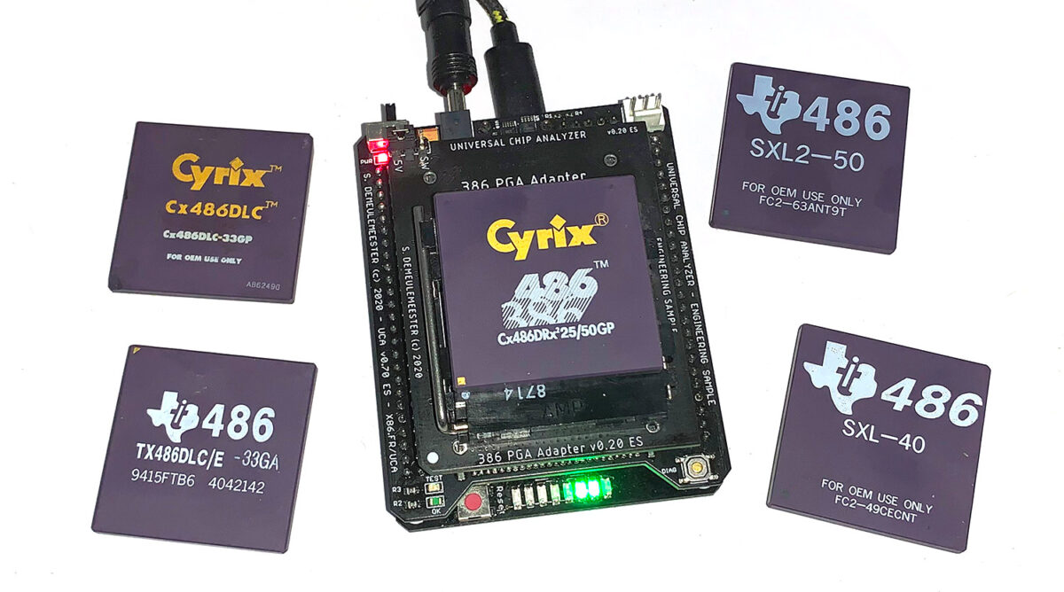
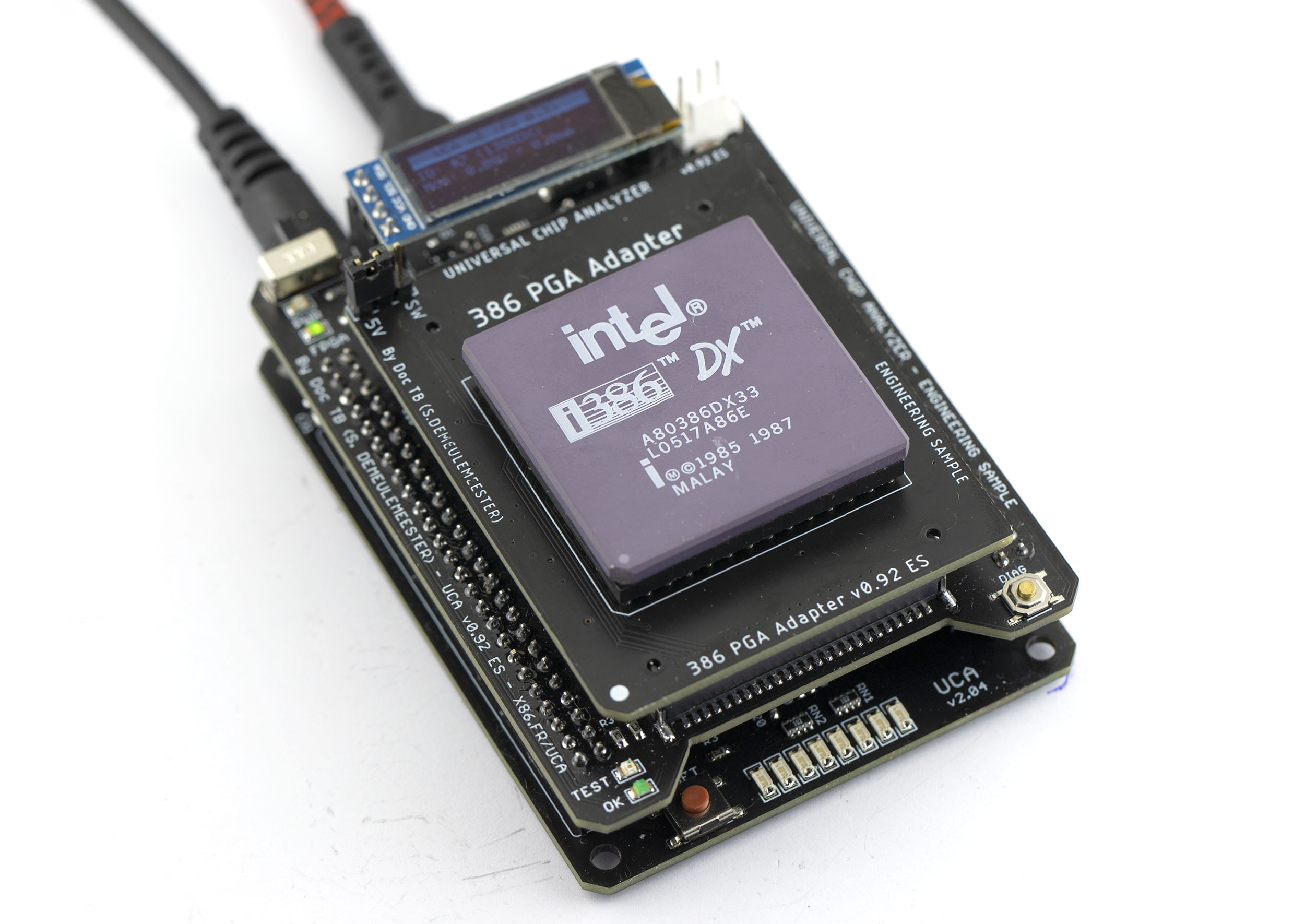
 The 386 Adapter has been the most difficult one to build so far. While the hardware is now almost fine, it still need some work on the FPGA code to fine-tune some timings.
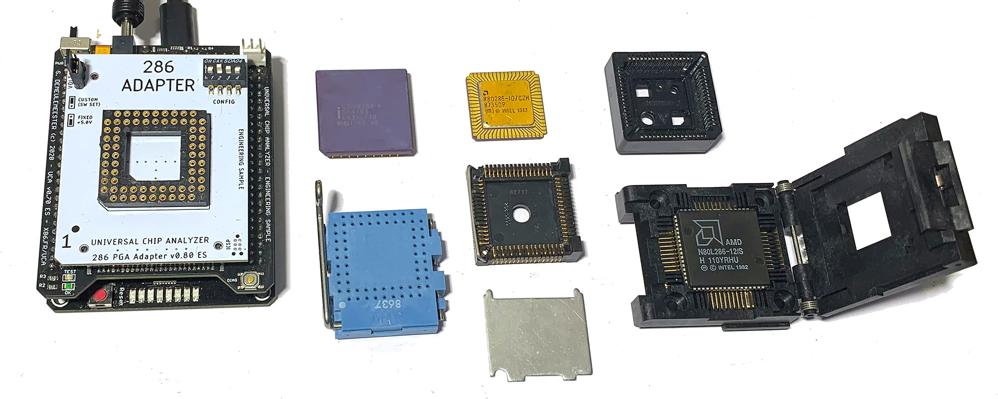
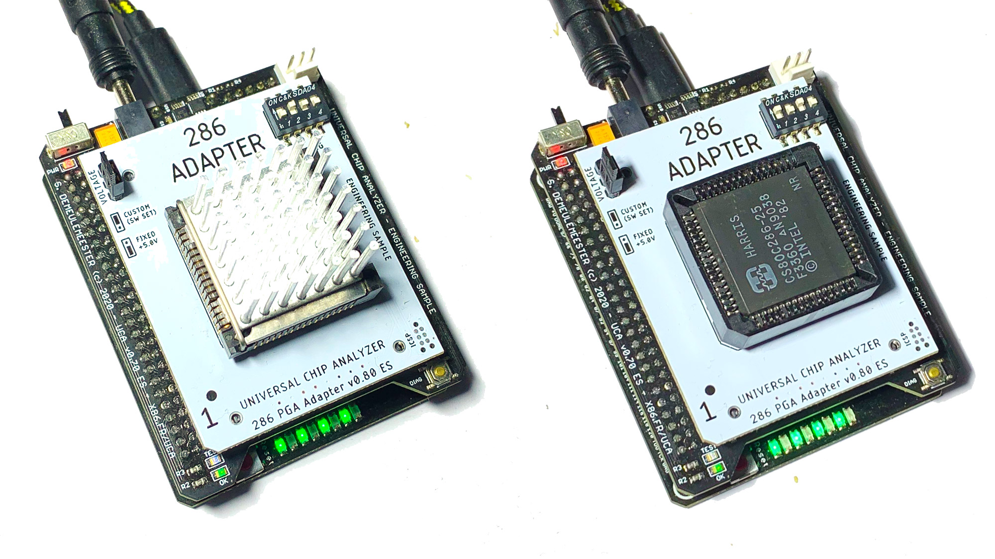
 Almost finished and working as expected with all kind of 286s. The internal MCU code must be rewritten to accomate the new communication protocol, but it’s not a very complex task.
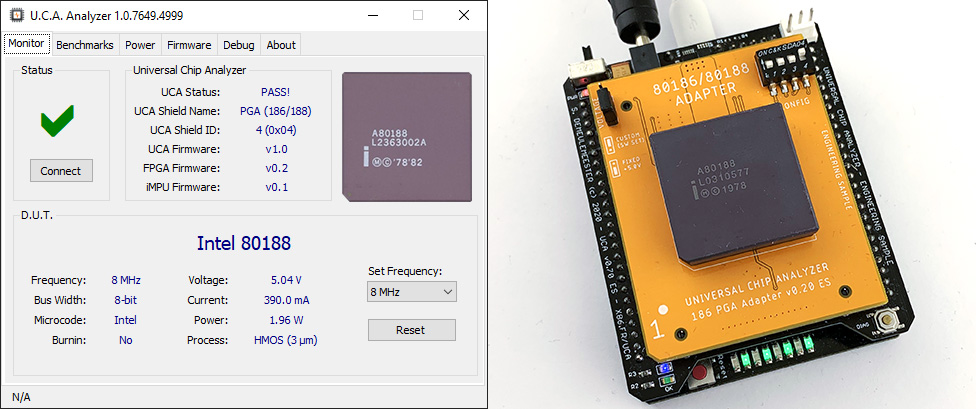
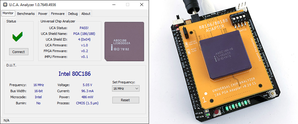
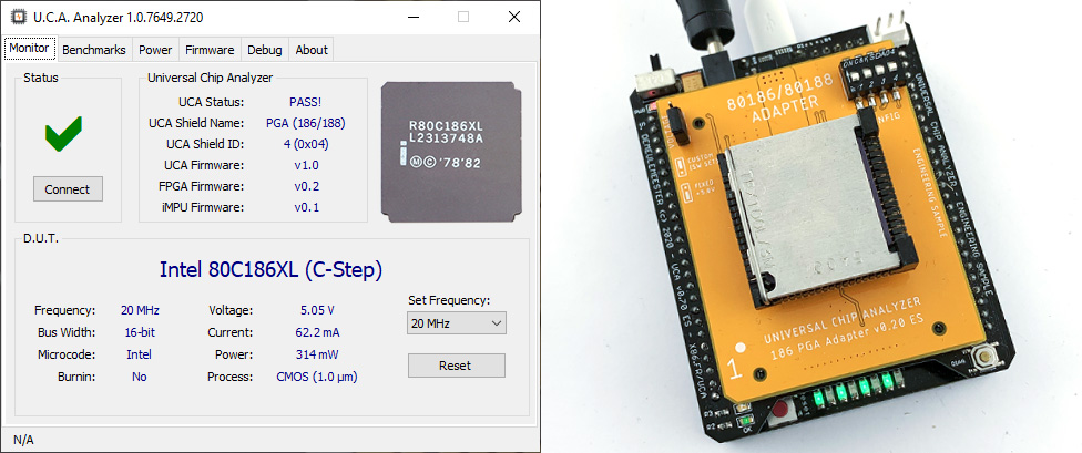
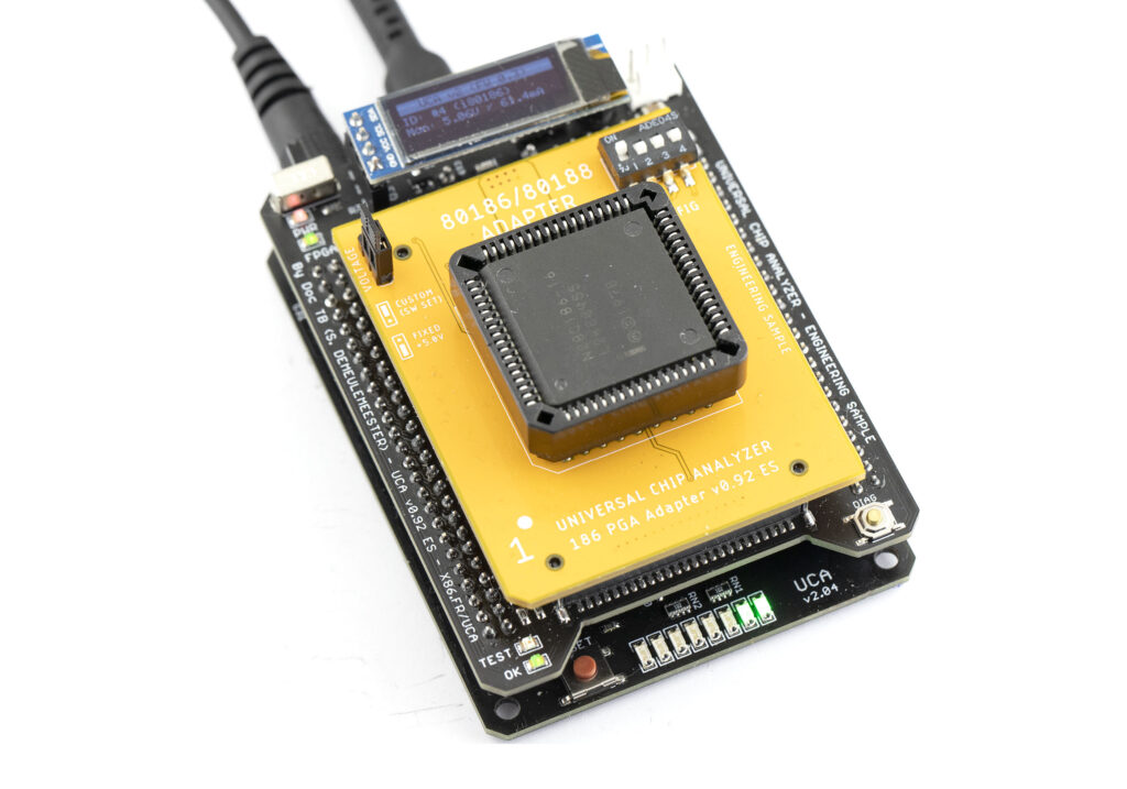 The 186 Adapter was the first adapter to be build directly for the new UCA “v2”. It was used to debug the new communication protocol between the different part of the UCA. Both Hardware and Software are now done. The only missing feature is the automatic detection of 186 vs 188 (currently, you have to select the correct bus type with the DIP Switch)
-
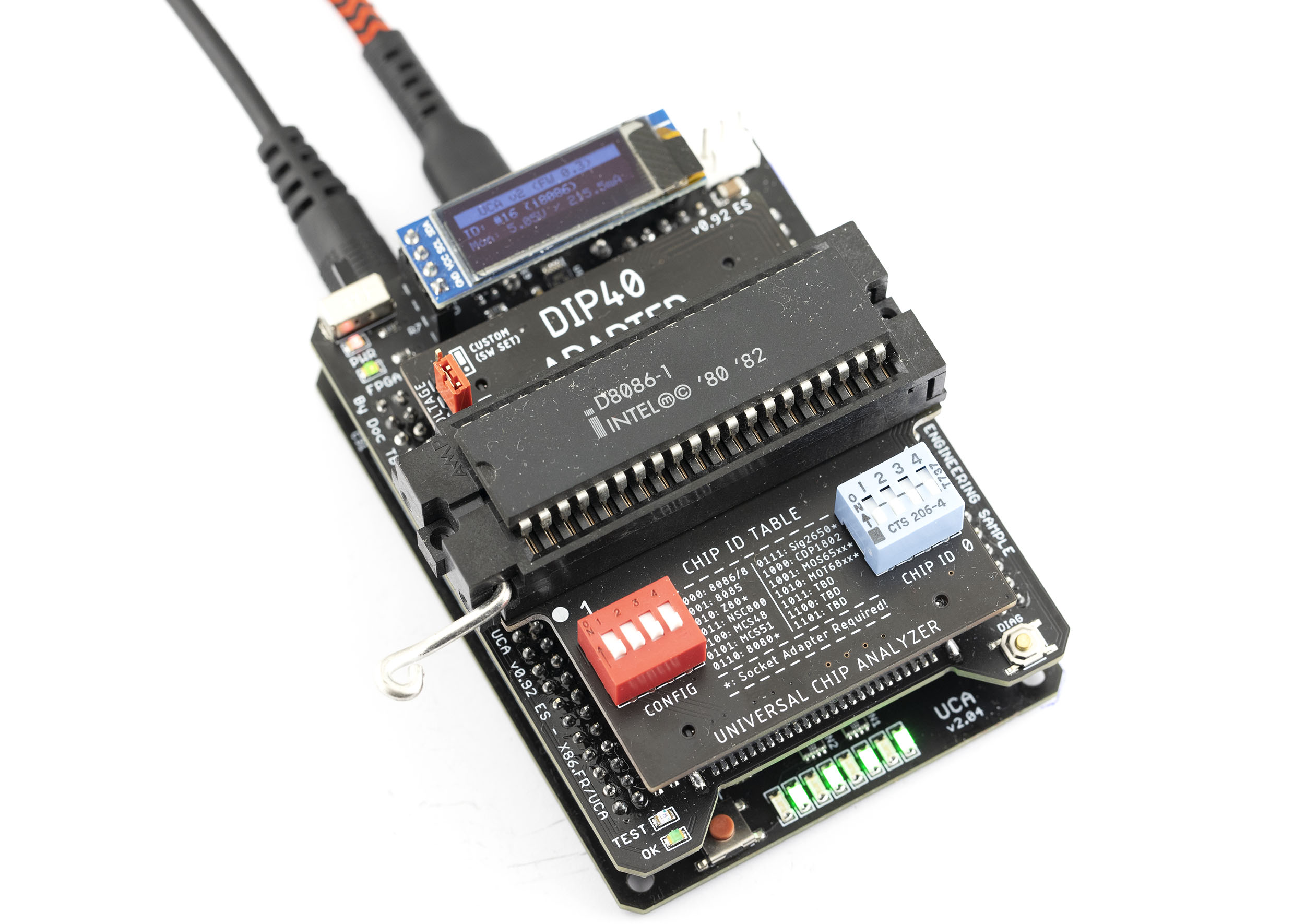
- UCA DIP40 Adapter (8088/8086 & more)
 The “iAPX-86 Adapter” has been renamed the “DIP40” Adapter as it is able to also test various other DIP40 IC. Along 8086 & 8088, the UCA DIP40 Adapter can also test 8085s, NSC800s, MCS48 and MCS51 MCUs, RCA “COSMAC” CDP1802s without the need of any adapters. With a specific adapter that plug on top of the DIP40 ZIF, it can also test Zilog Z80s, 8080s, MOS 65xx and Motorola 68xx.
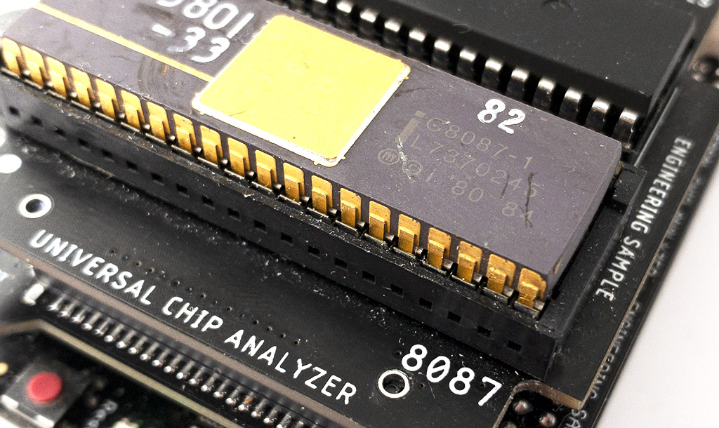
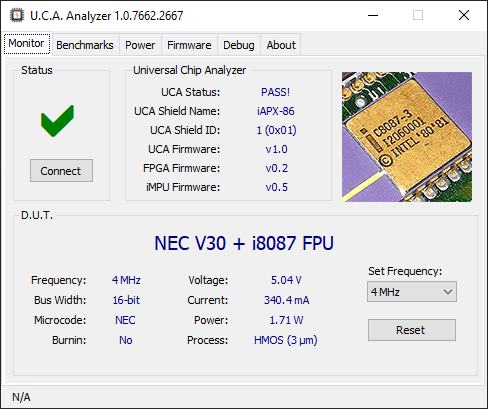
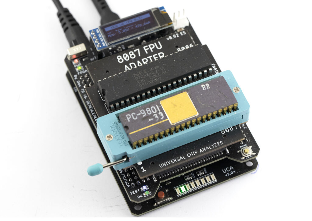 The 8087 Adapter has been quickly developed to show the UCA’s ability to also test FPUs. It requires a fixed 8086-compatible CPU that runs in MAX mode (while the DIP40 Adapter uses the MIN Mode).
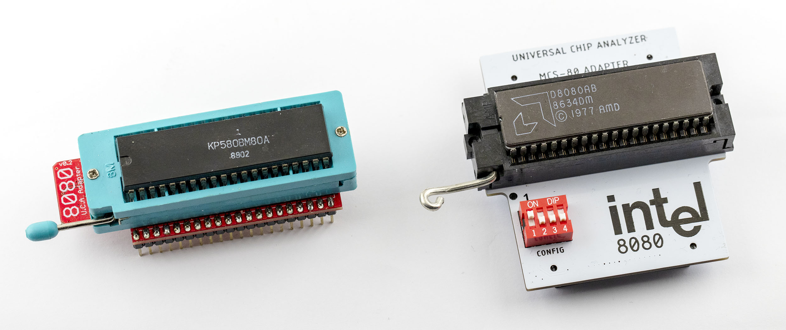
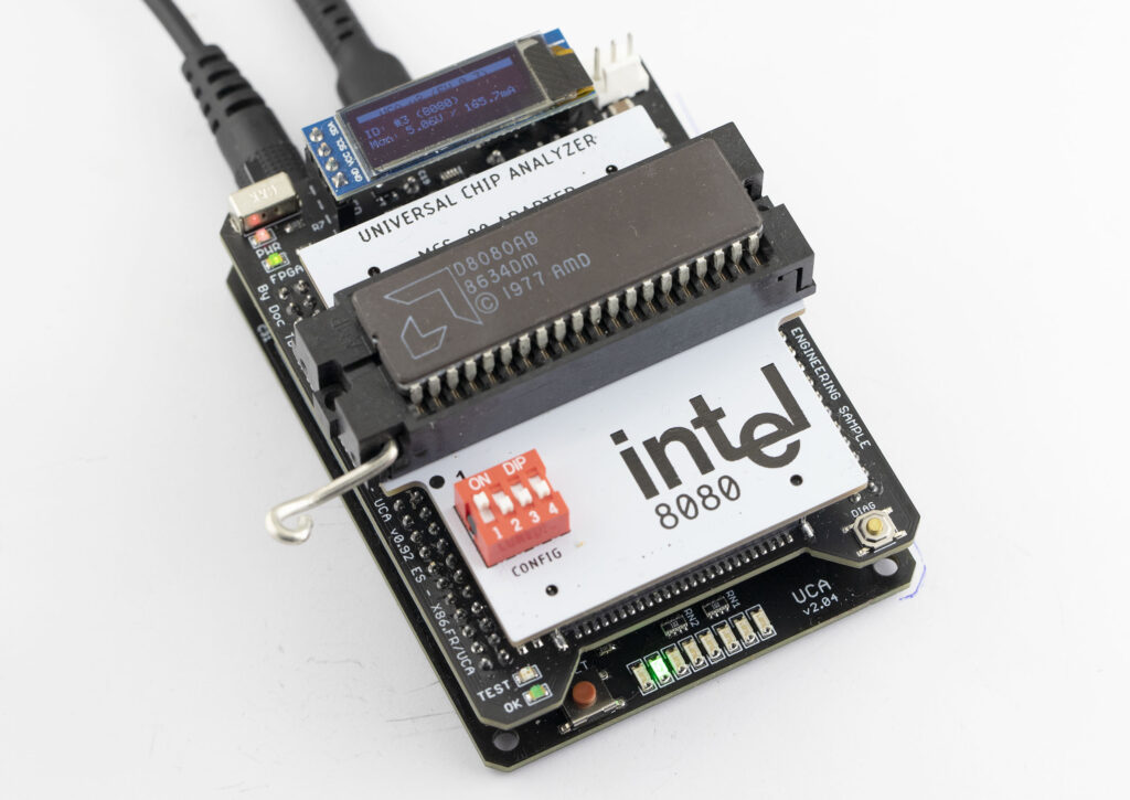 After discussion with fellow CPU collectors, I developed a standalone adapter for Intel 8080s. The price and feature of this one are the same than the Adapter that fit on top of the DIP40 Adapter :

At this time, I’m sure witch solution is the best. Maybe the standalone version is better to avoid mistake with DIP Switches… Leave a comment to give your thoughts!
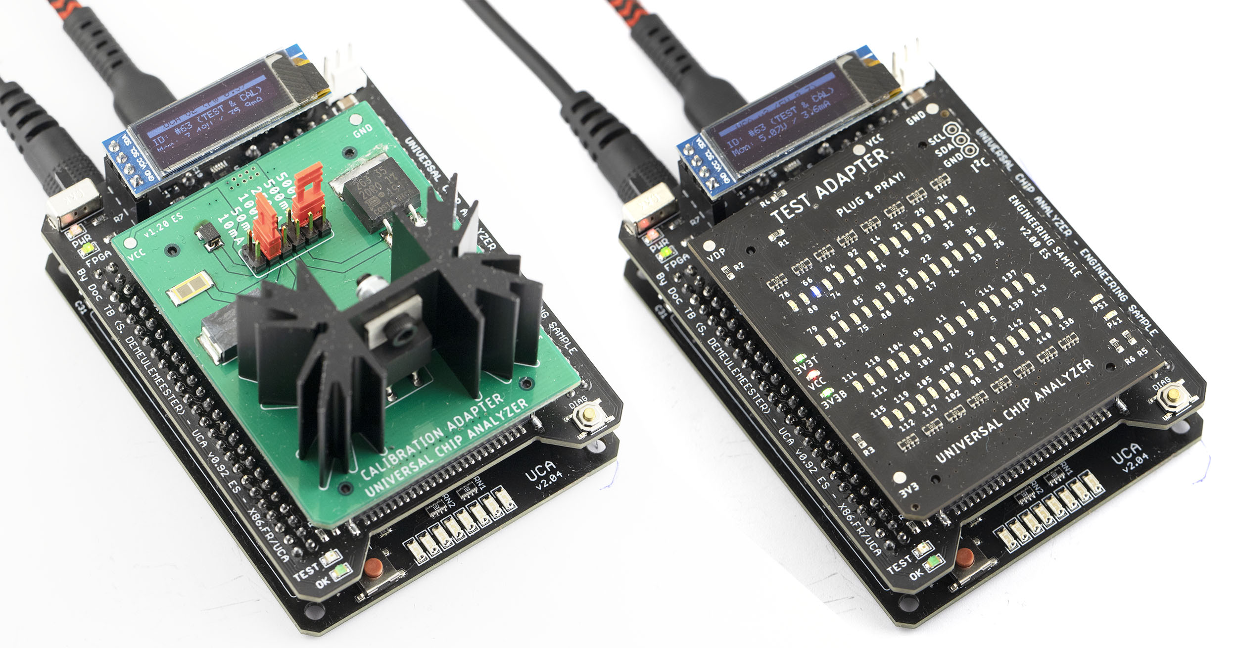
These Adapters are just for internal use, but I wanted to share some pictures just for fun.
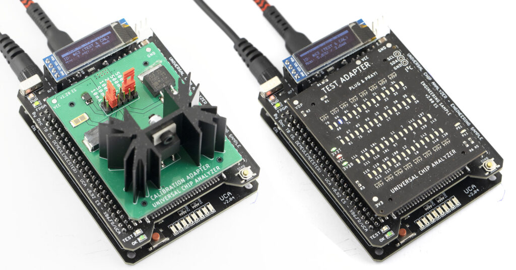 The left one is fitted with many precision power resistors and is needed to calibrate the power monitoring IC at various current load (10 mA, 50 mA, 100 mA, 250 mA and 2×500 mA). The right one is mainly used to test all signals of a newly-assembled FPGA/IF boards. It can detect shorts to VCC, open-circuits or adjacent-signal shorts. A backplate “Firmware Programmer” board with tiny pogo-pins has also been developed to flash the initial bootloader inside a blank UCA.
Stay tuned for more news about IC support and UCA production soon!
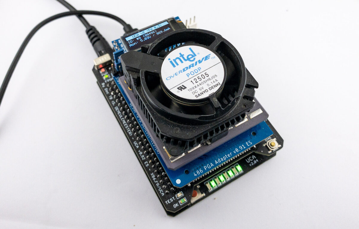
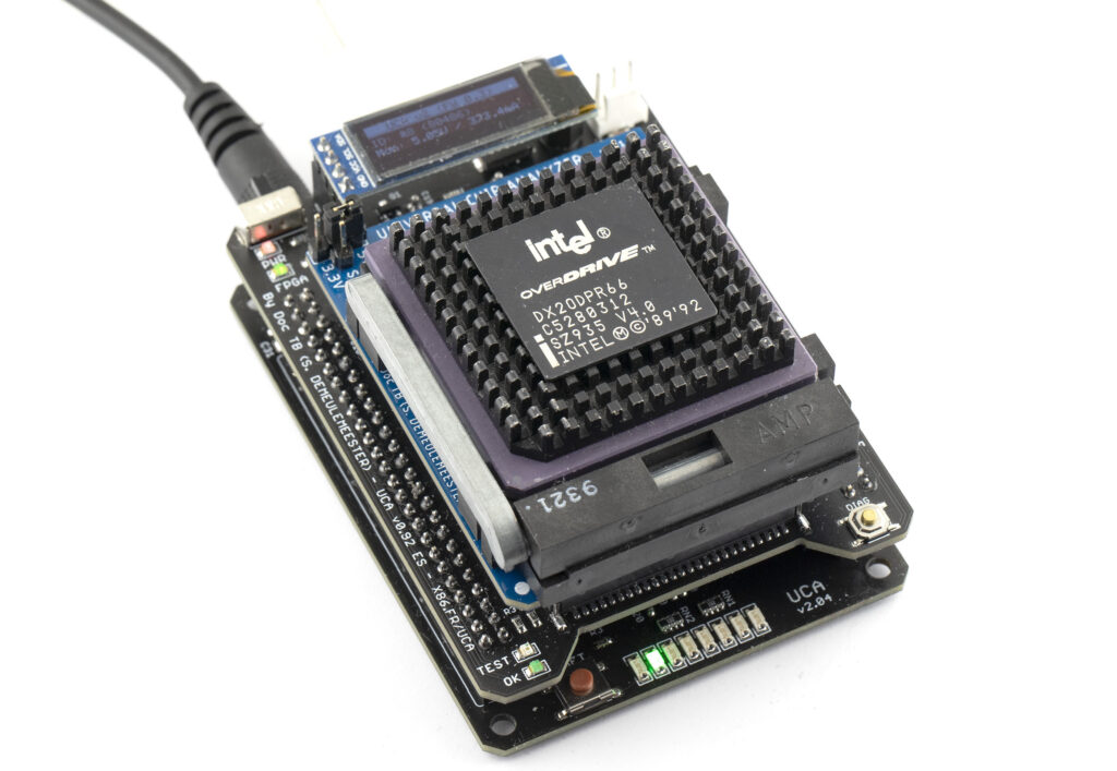
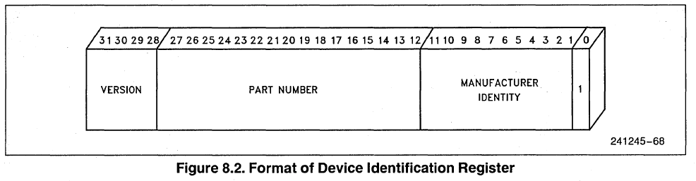
 As we can see, all pins but 8 are reserved (No connection) or used for power supply (VCC/VSS). Pentium ODs requires much more power than any 486, so Intel basically doubled the number of power supply pins to insure stability. The INIT (F19) pin is basically useless because it’s redundant with RESET and supplied with an internal pull-down to avoid spurious trigger. The 7 others pins are related to Write-Back L2 cache, which is useless on the UCA because the internal RAM is as fast as the L1 cache. So maybe the Pentium OD can work without connecting the outer rows?
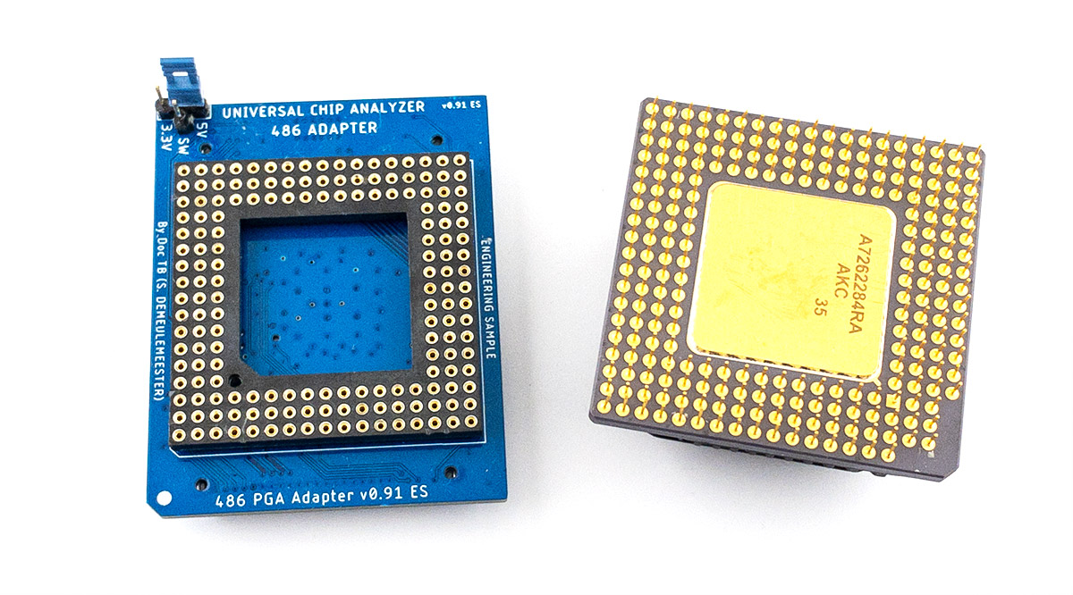 The Pentium Overdrive 83 MHz fits perfectly with the outer pins floating.
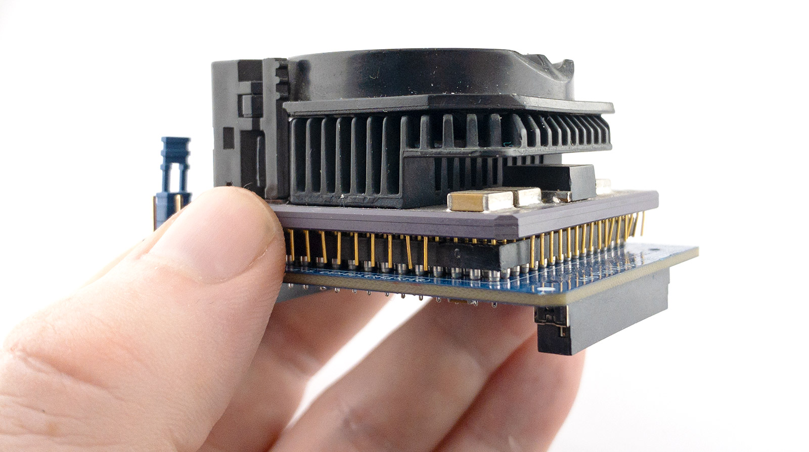
 After adding some code to support the new CPUID (0x1532), the UCA Analyzer tool was able to detect the Pentium Overdrive correctly and run the full test suite without issue.
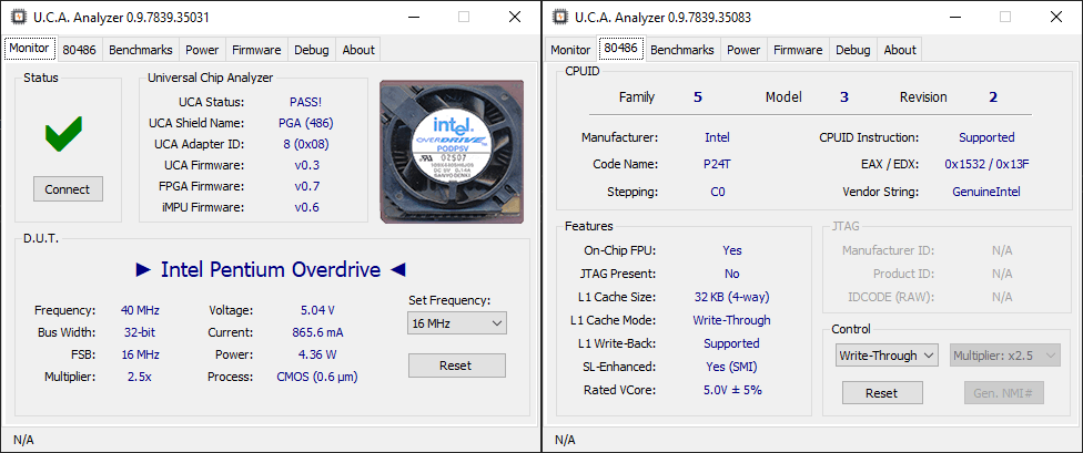 The Pentium OD doesn’t support JTAG, unfortunately. Power consumption is quite low for a Pentium-class CPU: 865 mA at 40 MHz. The last question is: how high can it go without the additional power supply pins connected? I tried 20 MHz FSB (50 MHz clock) without issue, then I tried 25 MHz FSB for a 62.5 MHz clock (like the Pentium Overdrive 63 MHz)
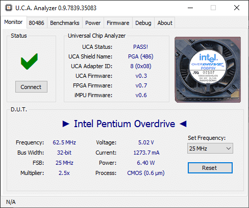 And it still works! Current consumption rises to ~1.3A to reach 6.4W. I also tried running the Pentium OD at full speed (33.3 MHz FSB for a 83 MHz final clock) but unfortunately, it only runs for a couple seconds before crashing. There is no doubt that the crash come from the missing power supply pins, but being able to run it at 63 MHz on the UCA is quite impressive!
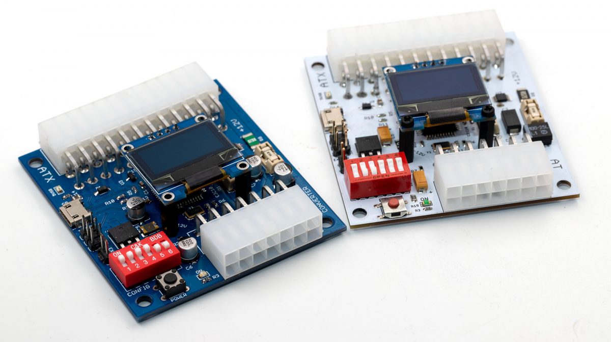


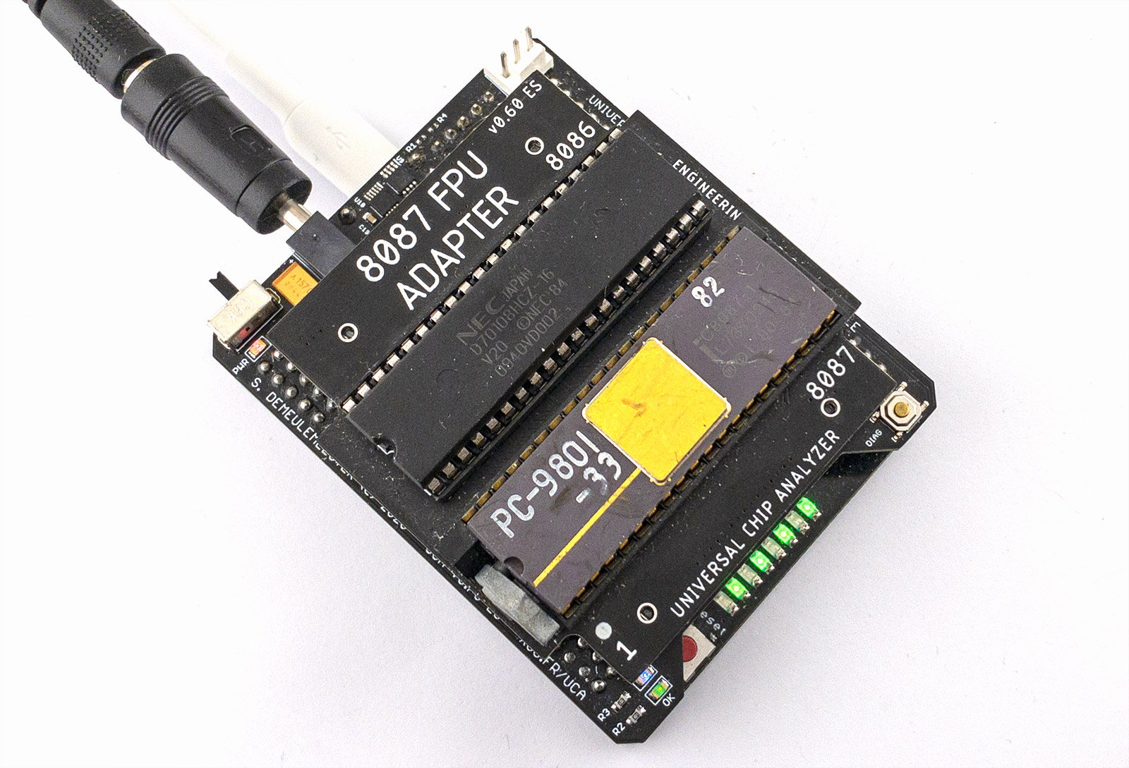
 An option to automatically subtract the power consumption of the 8086 (to show only the one from the 8087) will be added later . Target frequencies are 4, 6, 8 and 10 MHz.
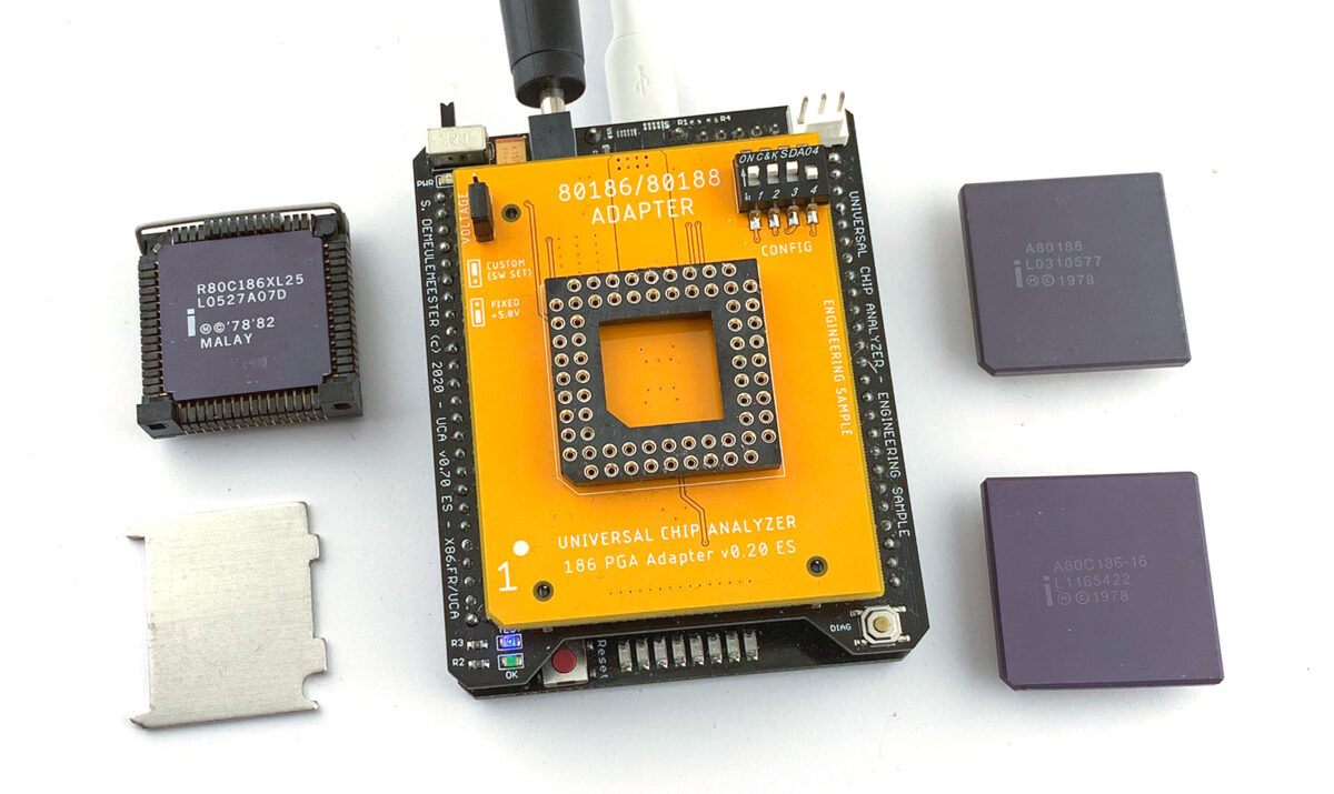

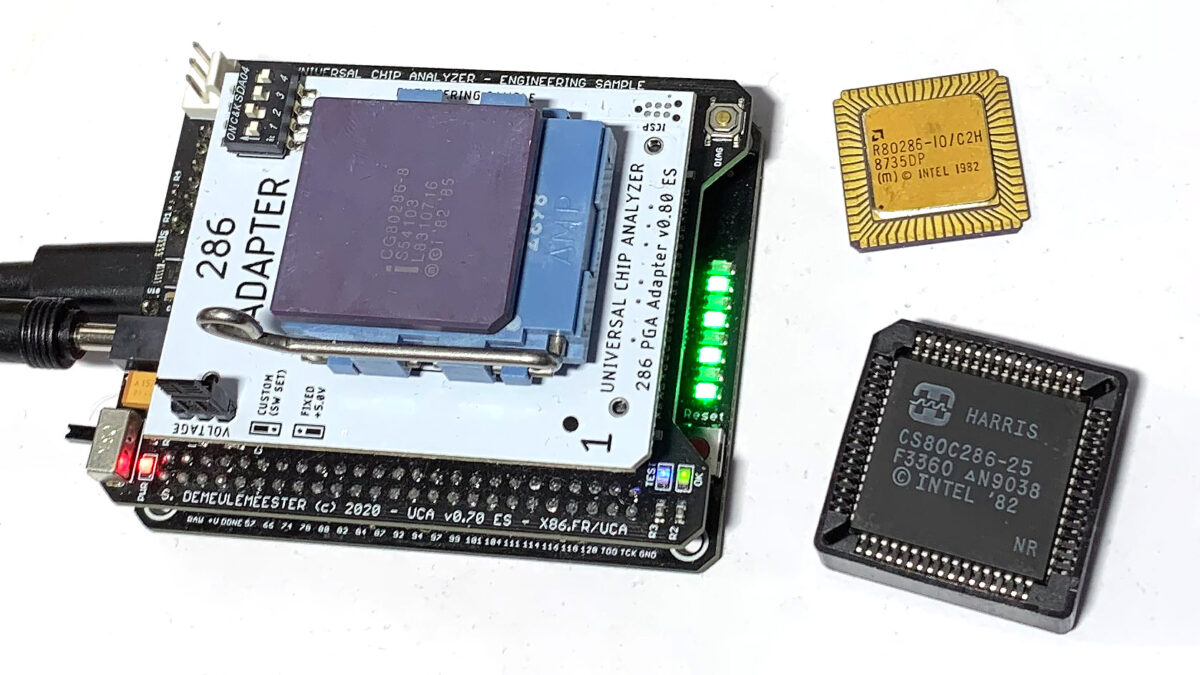
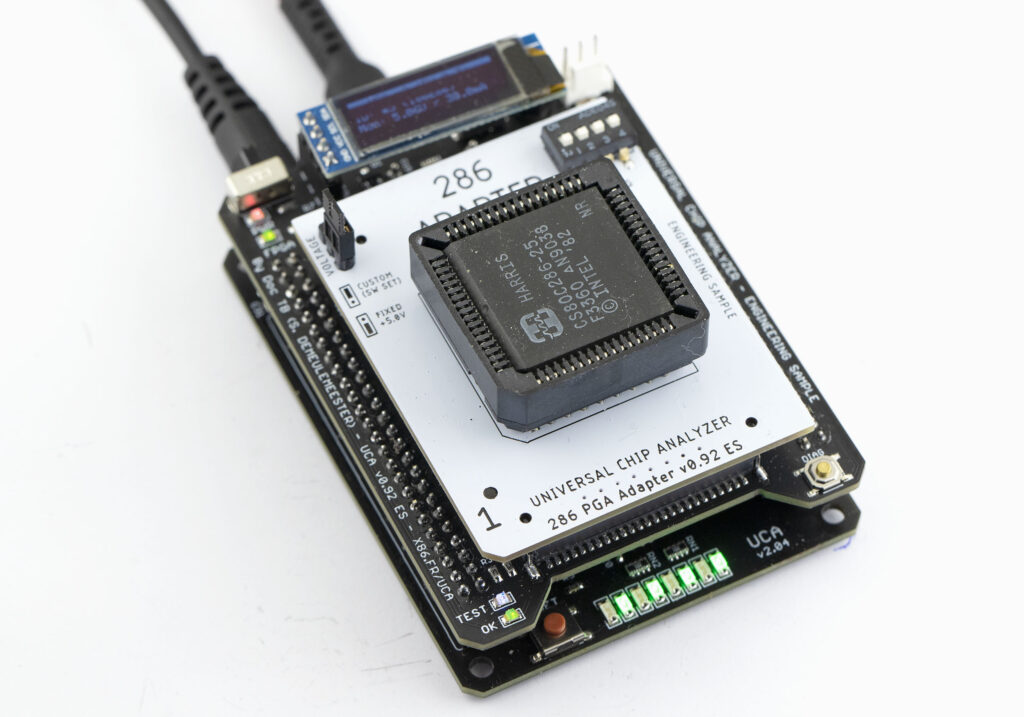
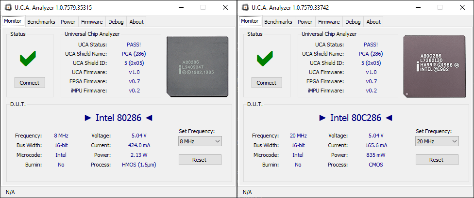 Why not 25 MHz? Because the 80286 requires a clock-doubled input and feeding a 50 MHz clock to get the 25 MHz core frequency would have required an external PLL. Not a big deal, but there is only one rare 286-class CPU that supports this frequency (the Harris/Intersil CS80C286-25 pictured above) and its timings is not fully compliant with the 286 specifications. Designing a special UCA adapter just for this chip is trivial, but quite useless because the 286 Adapter is already able to test it at 20 MHz. Speaking about “high” frequencies, using the right socket is crucial