In the 90s, Texas Instruments (TI) manufactured some 486-class CPUs under its own brand. TI was one of the third-parties who produced Cyrix processors (Cyrix was a fabless company). Consequently, the vast majority of TI-branded CPUs were just rebranded Cyrix 486s in PGA132 (386 pinout) or PGA168 (486 pinout). But Texas Instruments also designed its own 486 micro-architecture: the short-lived TI486SXL.
Good news: the Universal Chip Analyzer with the 486 adapter now supports all TI 486s!
Let’s start with the fastest one, the TI486DX4-G100-GA.
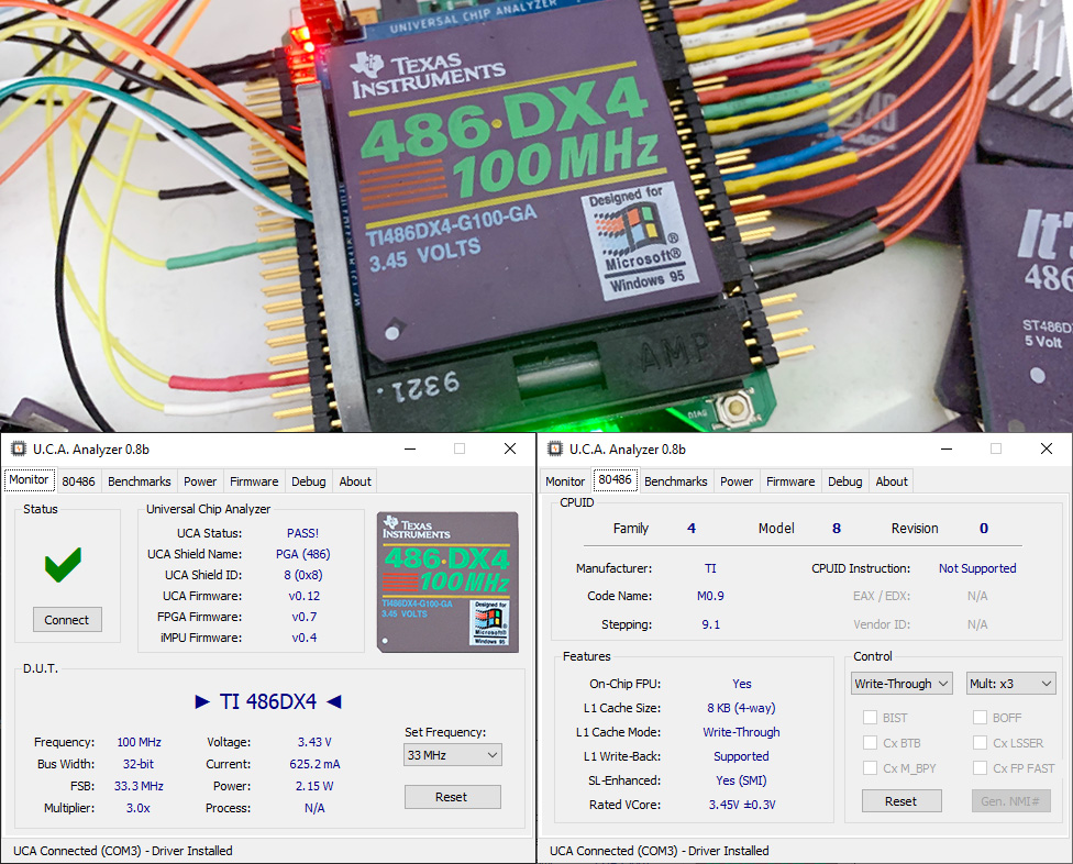 The “Colorful” Ti486DX4 is a rebranded Cyrix 486DX4-100: clock-tripled with 8KB L1 WB cache. Compared to IBM 486DX4 or ST 486DX4, both also rebranded Cyrix, the Ti486DX4 includes a tiny difference. IBM and ST CPUs are indistinguishable from a Cyrix CPU. Texas Instrument insisted to add a way to distinguish their CPU. This was implemented by setting a bit (DIR1[7]) in one of the Cyrix-specific registers. If the bit is “1”, the CPU is Ti-branded. If the bit is clear, it’s a Cyrix, IBM or ST 486. Other than that, nothing changed.
TI also released some 486 DX2, like this TI486DX2-G80-GA.
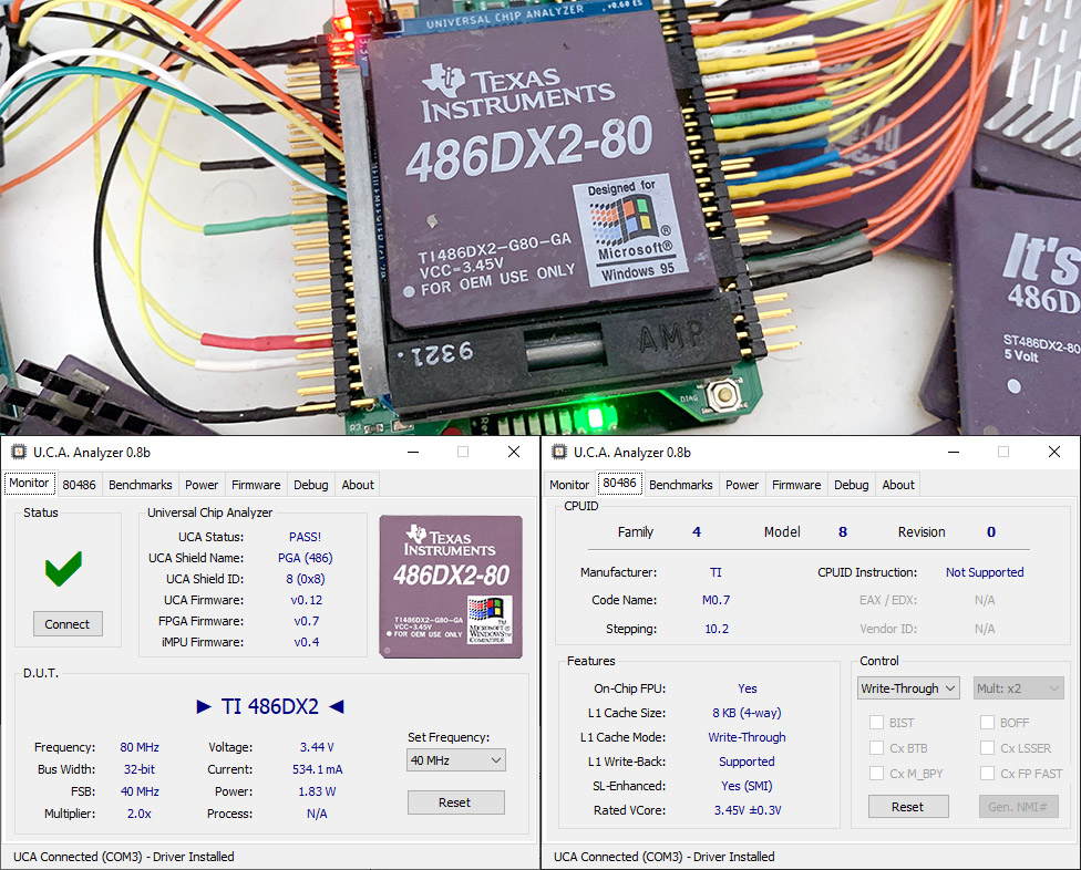 Again, it’s just a rebranded clock-doubled Cyrix 486DX2 with a specific identification bit set. The DX2-80 seems more common than the DX2-66. The Universal Chip Analyzer is perfectly able to test it at 2×40 MHz.
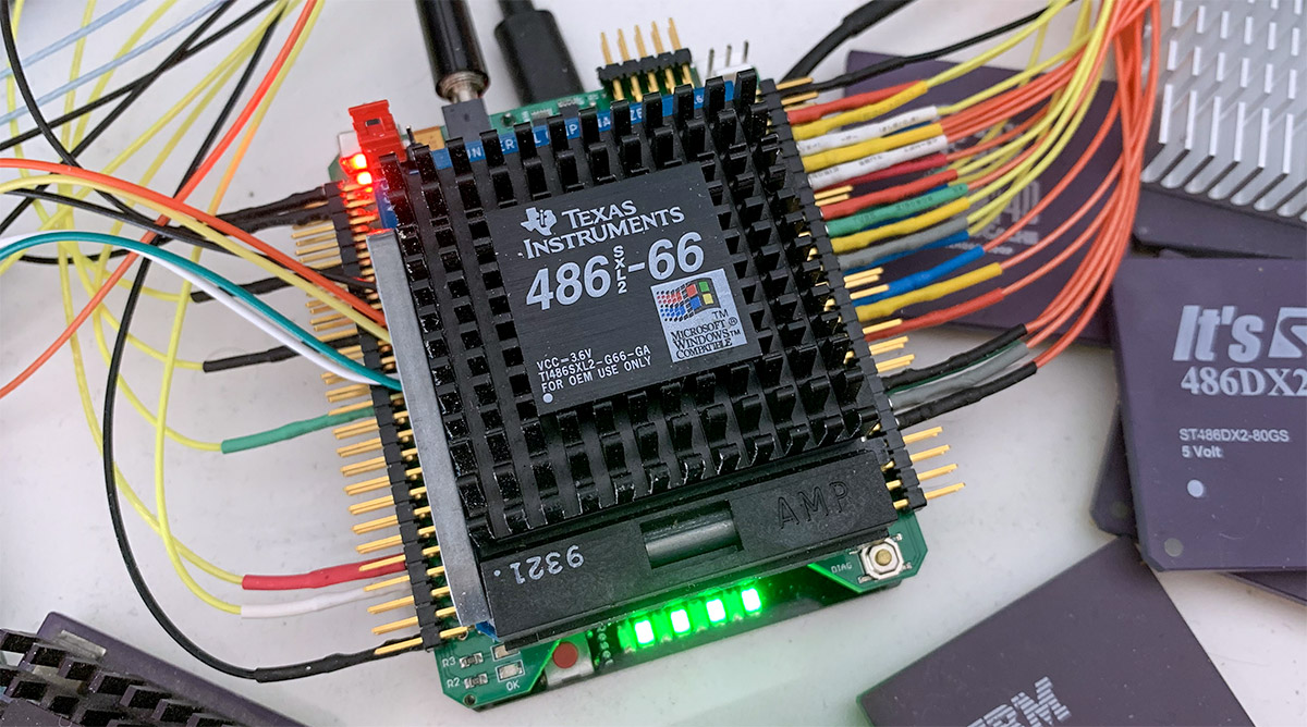
But the most interesting Texas Instruments 486s are the ones based on their own micro-architecture like this TI486SXL2-G66-GA.
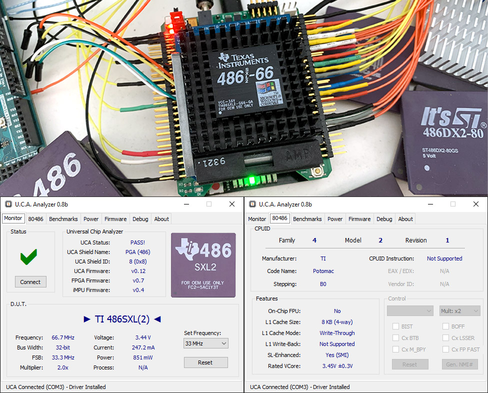 Codenamed “Potomac”, this clock-doubled CPU with 8KB of L1 cache doesn’t integrate a FPU. Ti was probably thinking of developing a FPU later. The mechanism to enable the clock-doubled PLL is different than all other CPU, who uses a specific pin to toggle between 3x and 2x (DX4s) or just boot at 2x by default (DX2s). The Ti 486SXL2 powers up in the non clock-doubled mode. To enable the 2x PLL, you have to write a specific bit in a proprietary register called CCR0 (with the same mechanism involving reading/writing to port 0x22h/0x23h as on Cyrix 486s). Setting bit 6 on CCR0 switchs on the clock-doubling PLL instantly (within 20 µs). I was able to overclock this CPU to 80 MHz at 2×40 MHz (still at 3.45V).
Texas Instruments also released non-clockdoubled “Potomac” CPUs like this Ti486SXL-40.
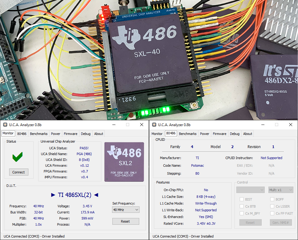 As you can see on the UCA Analyzer screenshot, it seems there is no way to distinguish them from SXL2 from a hardware point of view. Of course, it’s possible to check if the CCR0 bit 6 is set to 1 to know if clock-doubled mode is enabled, but the SXL2 can also work as a SXL in 1x mode.
While messing with CCR0 and the x86 code that run on the CPU, I found something very interesting: my SXL-40 also supports the clock-doubling mode! I had to run several benchmarks to be sure, but yes: that Ti486 SXL-40 can work as a SXL2 with the exact same power consumption and the same performances.
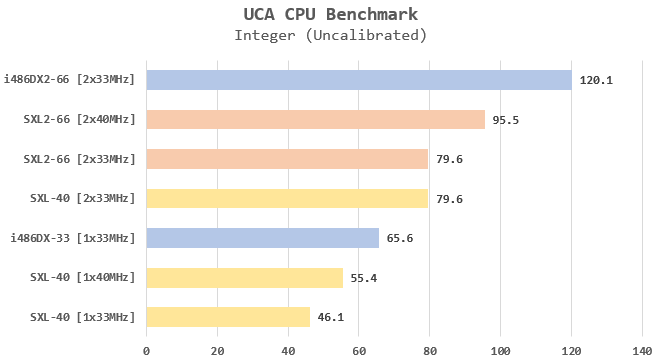
I used the preliminary Benchmark Mode on the UCA. These Integer scores are not calibrated so they’re only valid to compare these CPUs on a relative scale. We can see that the Ti SXL microarchitecture is ~30% slower than the Intel 486 one at equal clock frequency, but the SXL-40 is just 18% slower than a Intel 486DX-33. The Ti SXL2-66 is much faster then the DX-33, but the i486DX2-66 is far beyond.
Finally, it seems the SXL and SXL2 – at least on B0 stepping – are the exact same CPU. The B0 stepping is probably the only one that can work in 2x mode. “Potomac” A0 doesn’t support SMI and probably doesn’t have the integrated PLL. I also tried to activate the 2x mode and keep the 40 MHz FSB on the Ti486SXL-40 and … it works, actually doubling the performance (similar to a hypothetical “486SXL2-80”).