Adding support for Cyrix & TI 486s was supposed to be a matter of hours. It finally took almost one month and gave me many headaches. I almost burned everything to the ground several times in rage, begged for help from FPGA’s gurus who told me what I’m trying to achieve was like squaring the circle, but I did not give up. Let’s try to explain why it was so hard.
— always(@TLDR; Technical stuff) —
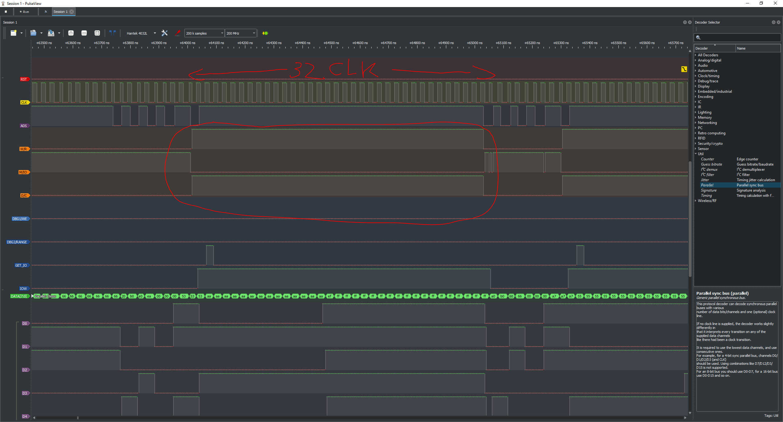
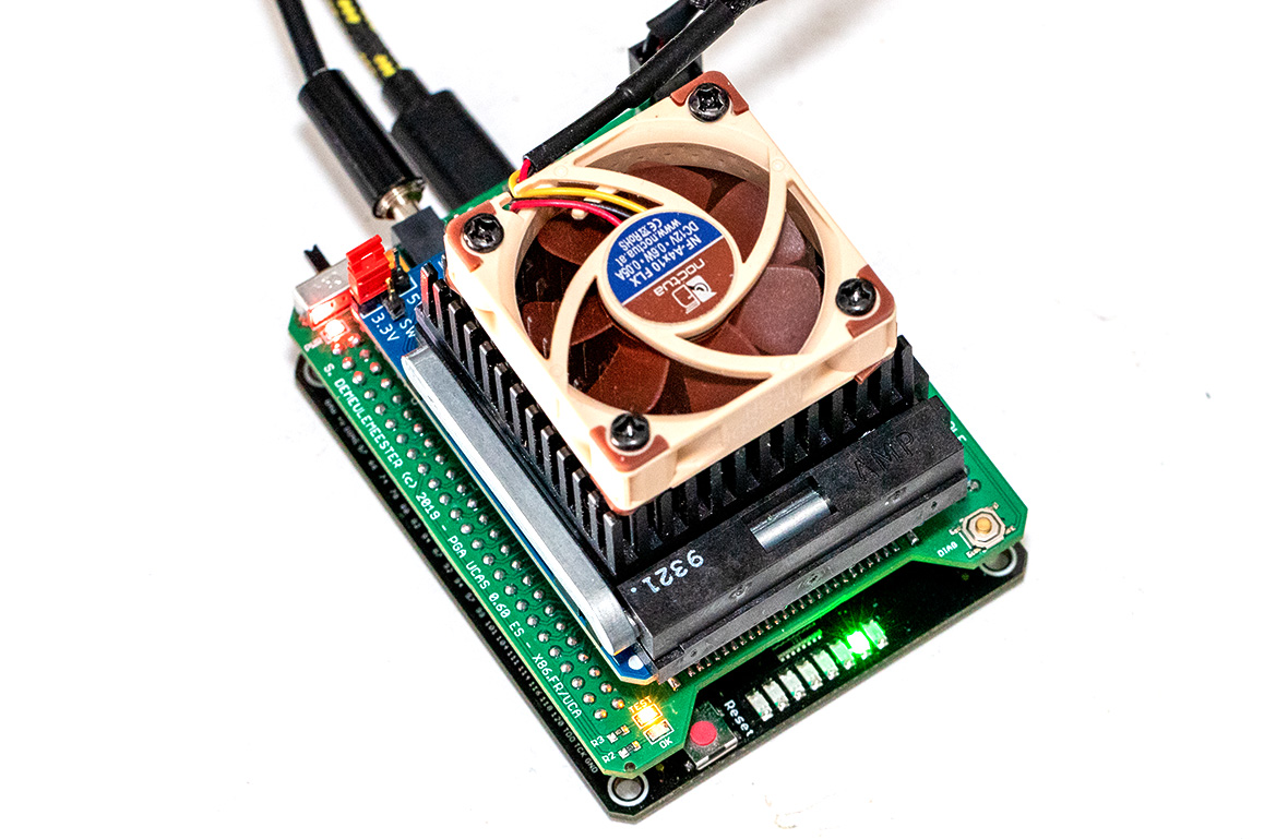
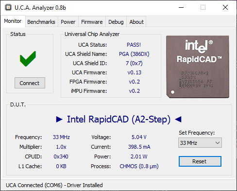
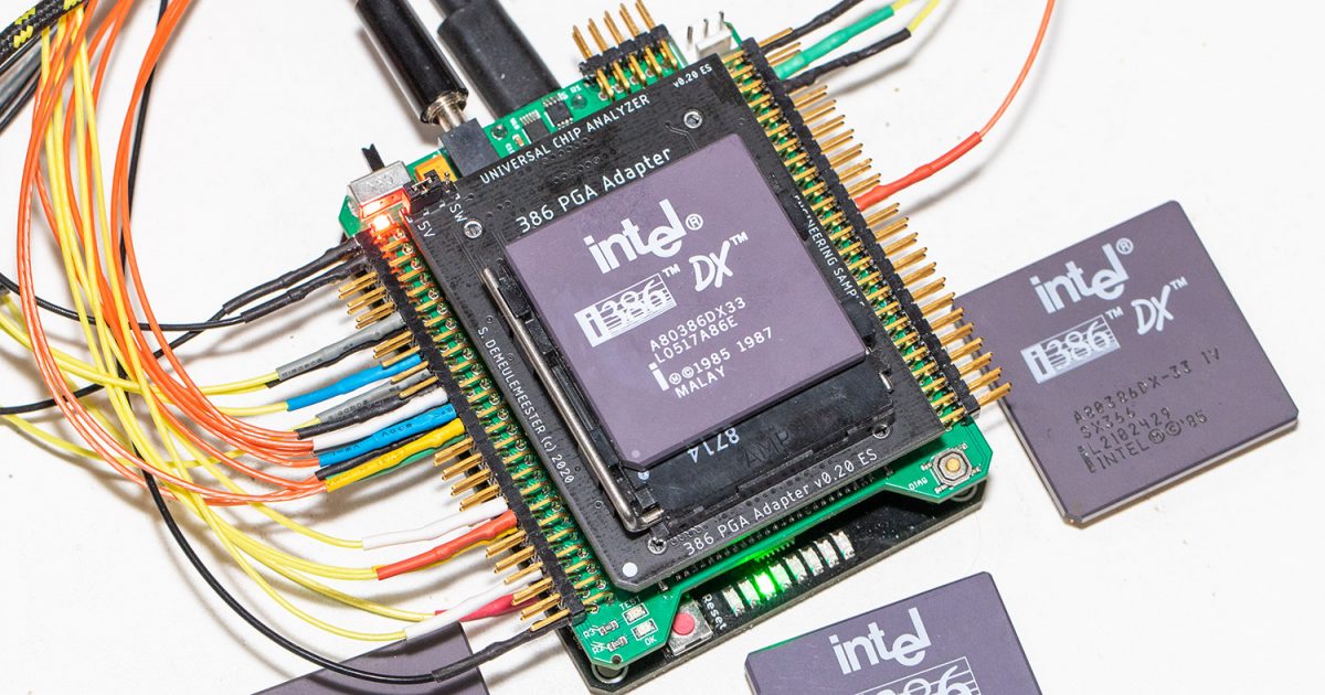
FPGAs are synchronous beasts used to create finite states machines: almost everything inside a FPGA is synchronized to a clock signal. Each time the clock is ticking, the HDL code analyzes inputs and sets a pre-defined state (that itself defines registers, outputs, the next state, …). To add support for a CPU, you must read the datasheet and write some HDL code that will provide the correct outputs (from the FPGA to the CPU) within the required timings. All these timings are linked to the base clock. A synchronization between the CPU and the FPGA is crucial. For all other CPUs I’ve worked on for the UCA, the FPGA provides the base clock to the CPU. Both the FPGA and the CPU are sharing the same clock and synchronization is easy. But 386s require a clock-doubled input (80 MHz for a 386DX-40 MHz) that I’m not able to provide directly from the FPGA because the 3.3-to-5 volt translators are too slow. So I use an external clock-doubler PLL, but doing so prevents the FPGA from having access to the CPU clock. That’s the root of all issues I had.
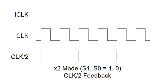
Fortunately, using an external phase-locked loop (PLL) means the clock input phase is synchronized with the clock-doubled output signal: the rising edge of both clocks occurs at the same time. Knowing the transmission delays added by the voltage converters at a given frequency, you can still synchronize your FPGA with the CPU without having access to the base clock. That works fine as long as you don’t change the frequency. But that was too easy: I want to be able to switch frequency on-the-fly and within a large range (from 12.5 MHz to 40 MHz to cover all 386s). That’s still possible if you build many bitfiles (compiled HDL “FPGA firmware”), one for each frequency. Nah! I want to use the same bitfile for everything, including support for both microarchitectures (Cyrix & Intel) despite the different timing’s requirements. That’s hell but I almost succeeded.
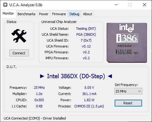
The actual firmware is not perfect but I’m quite happy with it because it works as expected in most cases. The remaining issue is a hole between ~21 and ~28 MHz where the FPGA can’t reliably catch the required inputs from the CPU at the rising or falling edge of the clock. My Logic Analyzer is unfortunately too slow to solve this but it’s not a big deal. The HDL code works fine at 12.5 MHz, 16 MHz, 20 MHz, 33 MHz and 40 MHz. The only “retail” frequency I’m not able to do is 25 MHz. I built another bitfile for this frequency only and I’ll hope to find a way to merge everything in the same bitfile later. To avoid losing my mind, I’ll wait to have enough money to buy a faster logic analyzer (like the lovely DSLogic U3Pro32) to work on this again.
— End —
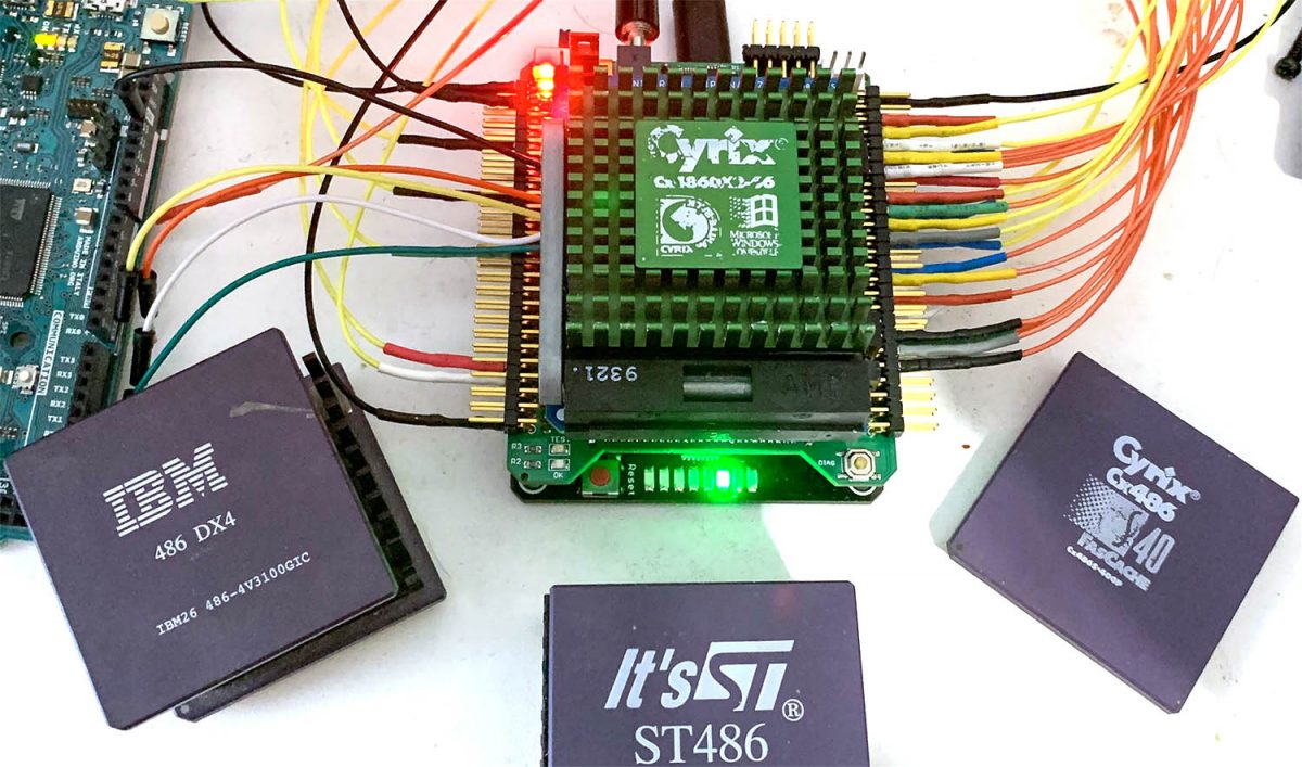
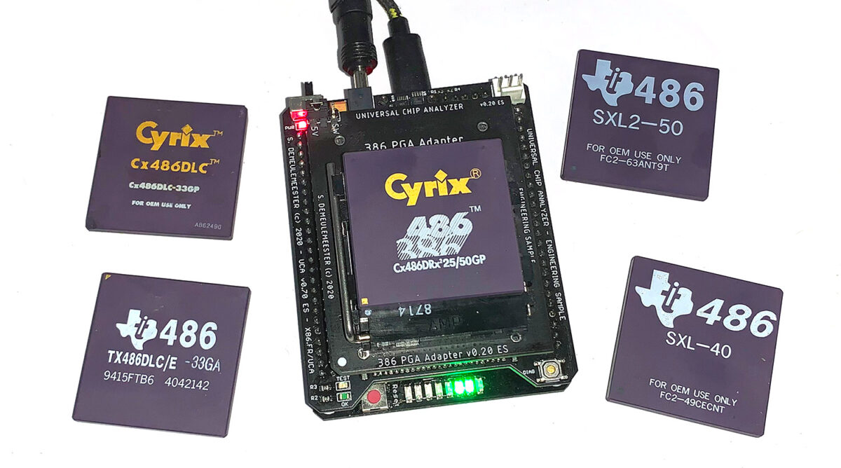
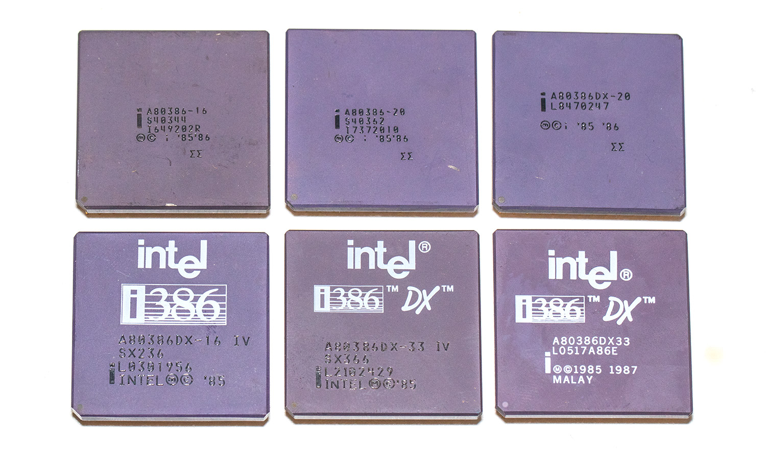
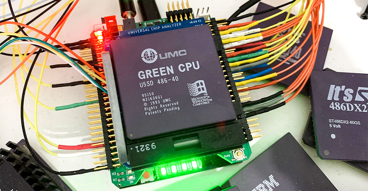
But here it is: the UCA supports all Cyrix-based 386 like the 486DLC. Here are the ones I used for the test:
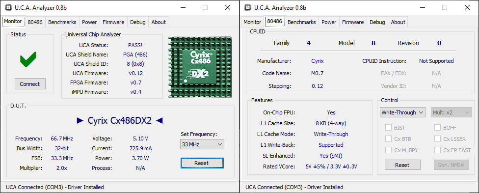
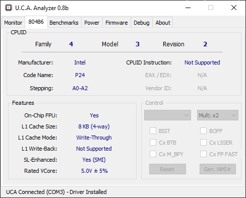
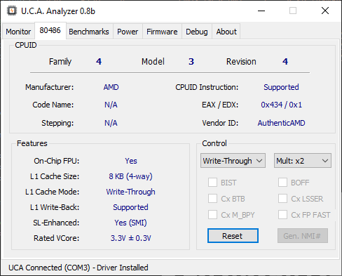
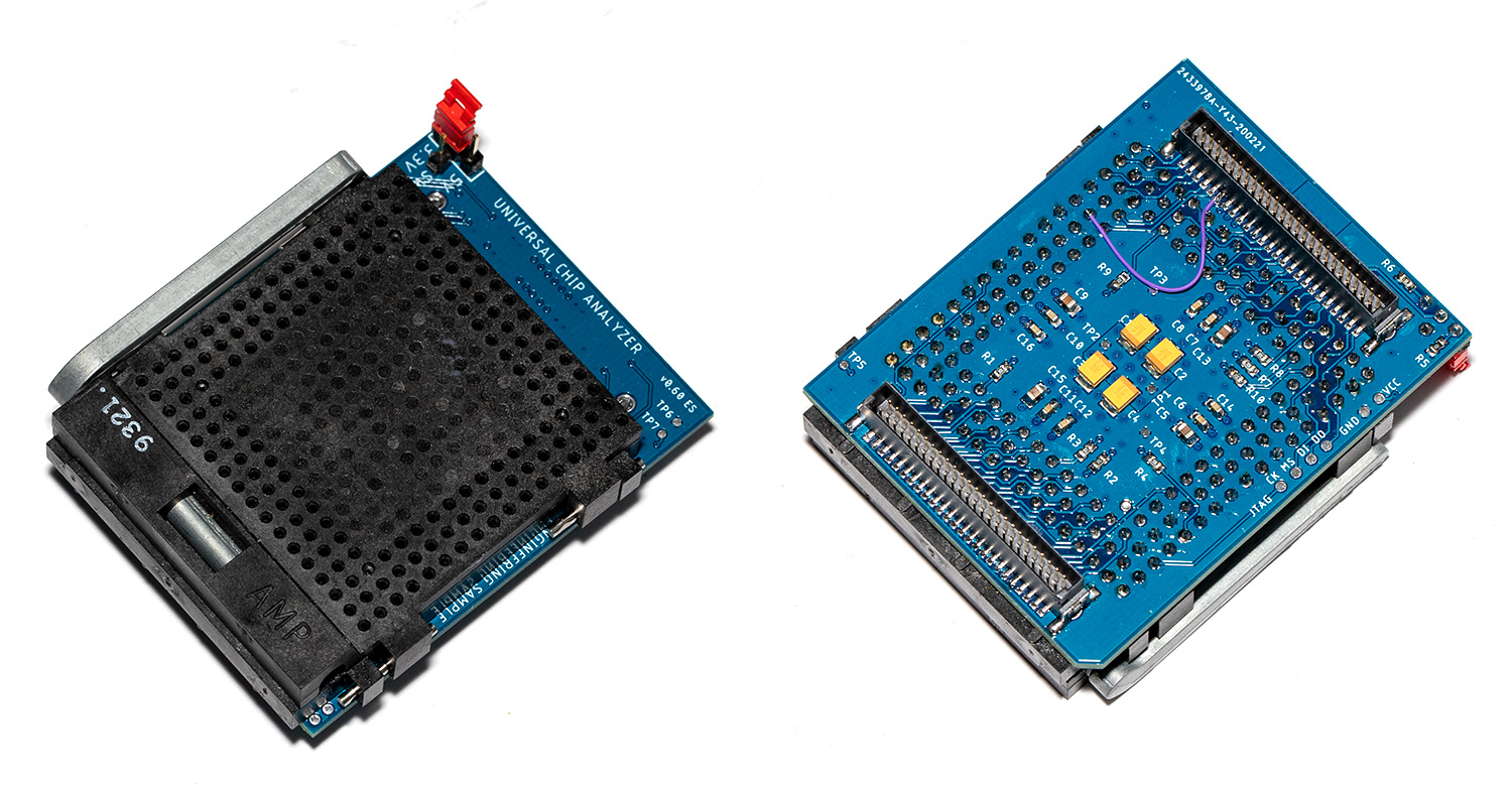
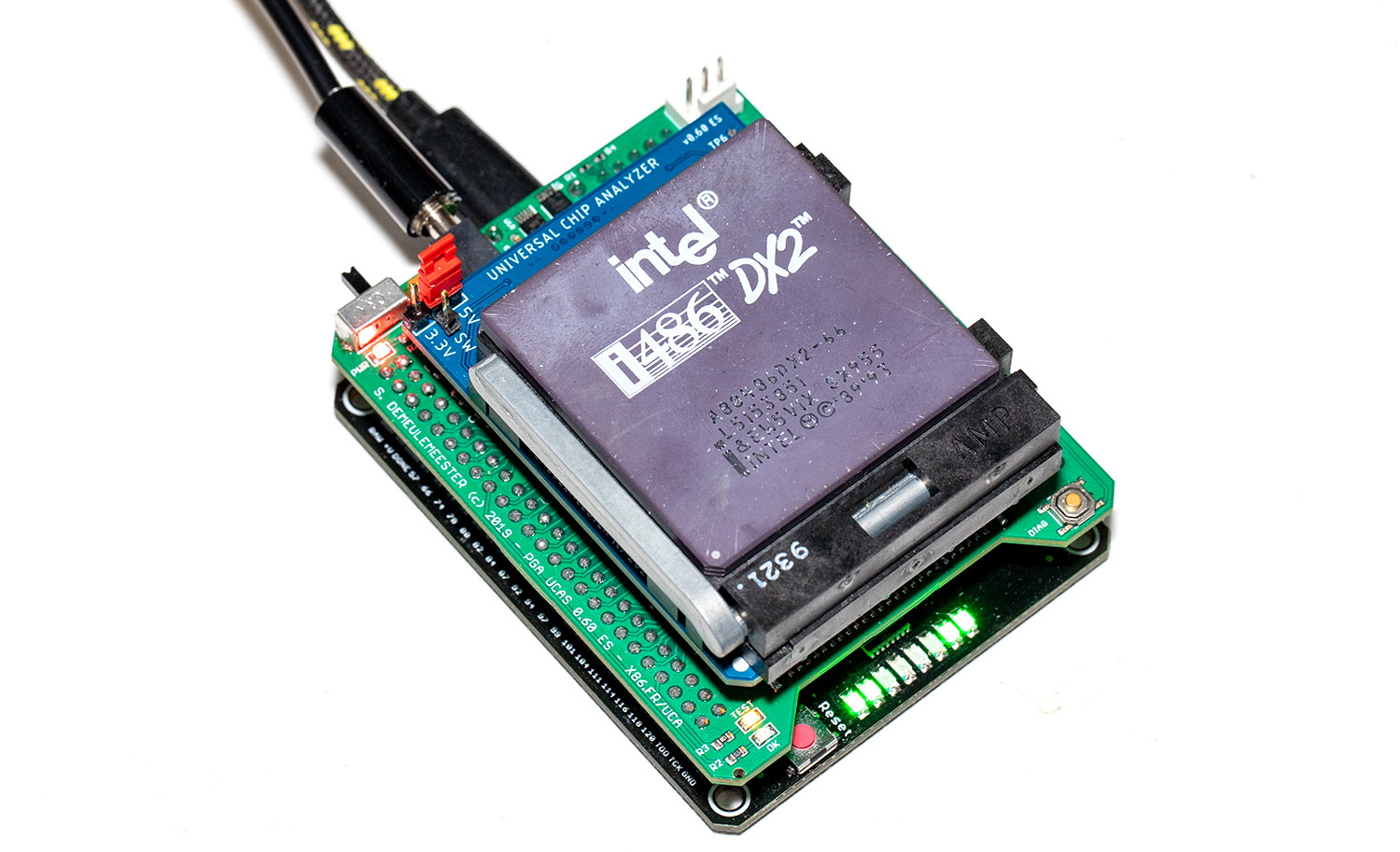
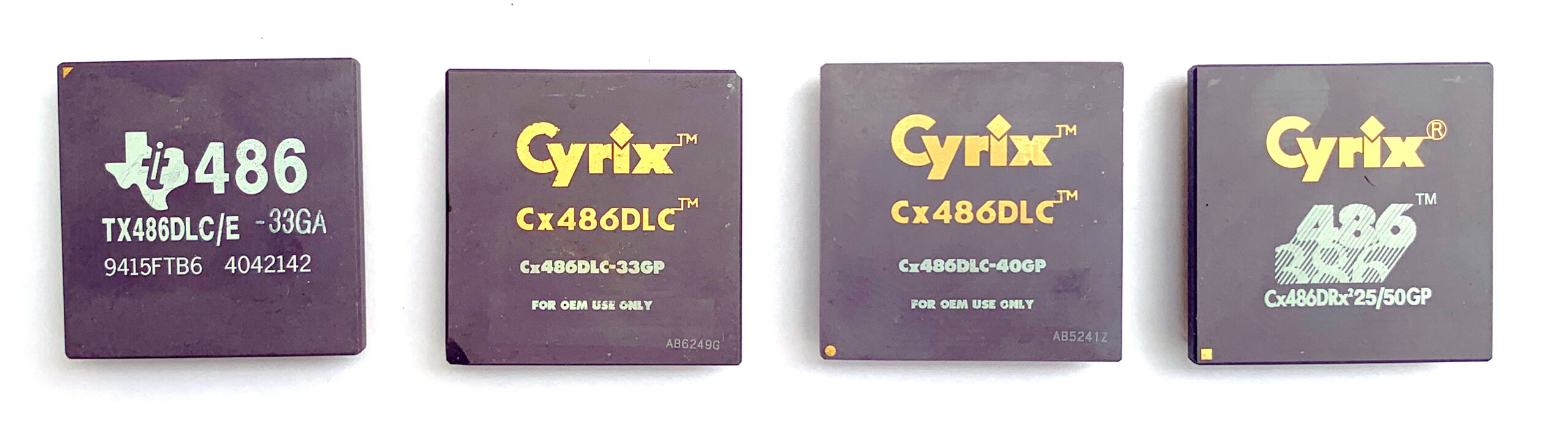 Unlike 386-class CPUs from AMD, which are based on Intel’s microcode and are exact clones, the Cx486DLC introduced in June 1992 uses a custom microarchitecture built from scratch by Cyrix. While still using the 32-bit 386 bus, they come with 486-class features like an embedded L1 cache and some new instructions. The Cyrix 486DLC is not a perfect pin-to-pin replacement for Intel 386s as timings are a bit different and cache control lines must be handled by the chipset. Compatibility issues are well known with many – especially older – motherboards. The original 486DLC was available at 25 MHz, 33 MHz and 40 MHz. All of these were manufactured by Texas Instruments on the 0.8µm CHMOS node. Ti also launched their own, rebranded 486DLC chips, which were exactly the same except for the marking. Please notice the vicious 90° rotation between printings and pin 1 on the Ti486DLC. Fortunately, the Universal Chip Analyzer have strong short-circuit protection built-in…
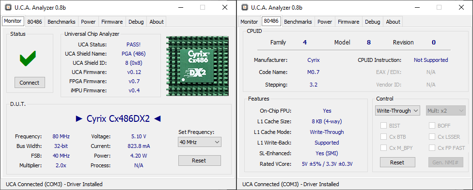
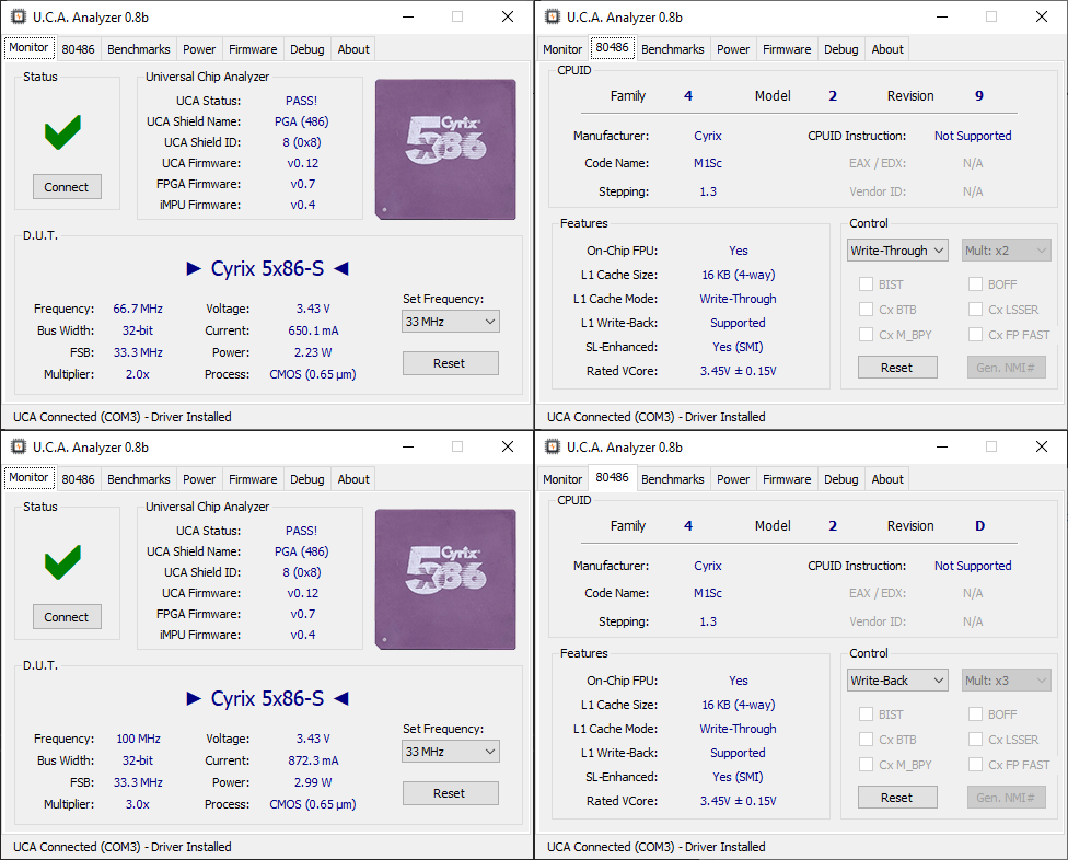
Cyrix also later released a special, clock-doubled version called the 486DRx². It was available at 16/32, 20/40 MHz, 25/50 MHz and even 33/66 MHz. This later one was the fastest PGA132 CPU ever released.

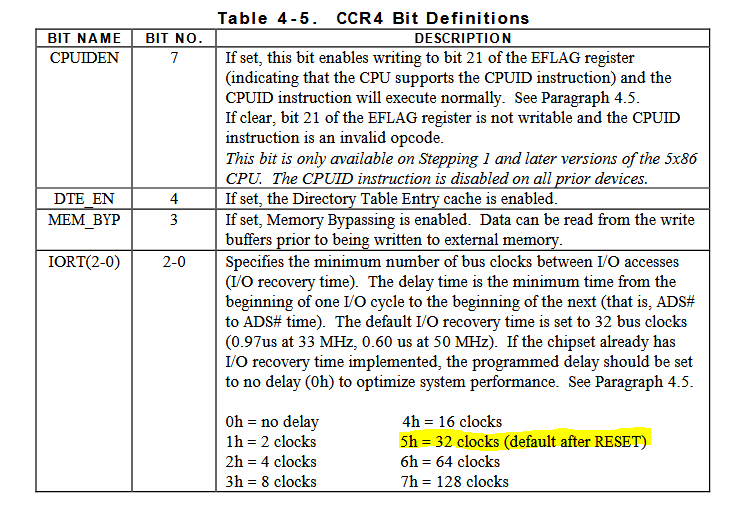
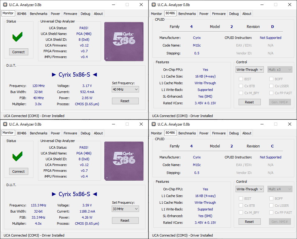
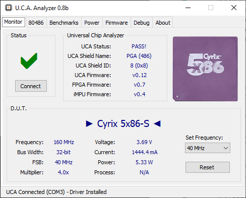
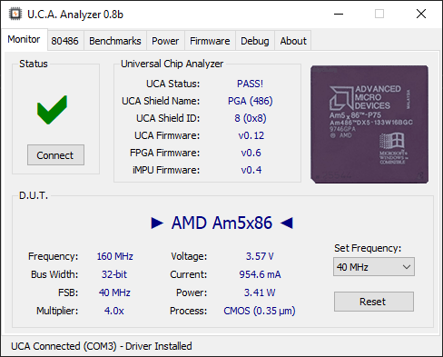
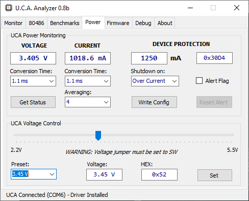
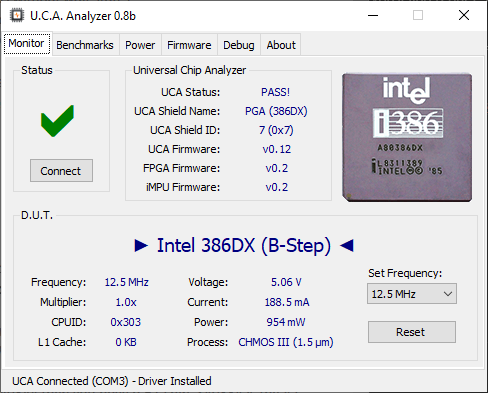
The original Cyrix 486DLC exists with two steppings: the earliest one with CPUID 0x420 and a later one with CPUID 0x421. The proprietary “DIR” identification registers available on Cyrix’s CPU is only available on newer CPUs. None of the 486DLC tested have them. The 486DRx² is the only one to have DIR registers and reports itself as Model = 0x07. The UCA happily tested the 486DLC at 40 MHz and was even able to overclock my 486DRx2 25/50 at 33/66 MHz for a short time. Cyrix 486s run hot and deserve a proper heatsink. Power consumption is as high as a 486 DX2 and can go as high as 4 watts (4 times higher than a later Intel 386 DX-33)!
Much later in the development process, I feel confident enough to try a blank 486DLC Engineering sample I got many years ago.
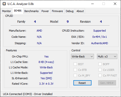
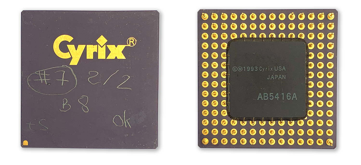 This ES is not a clock-doubled CPU like the DRx² and was able to run properly at 33 MHz. CPUID is 0x421 and – surprise! – it has DIR registers, identifying itself at Model = 0x01 (the expected value for a Cyrix 486DLC) and stepping 0x22, with seems to match the handwritten value (2/2) marked on top. The DRx2 25/50 tested above comes with stepping 0x21, so this ES seems newer. I don’t know at this point if any 486DLCs were released commercially with this stepping – or even if any retail 486DLCs have DIR registers enabled.
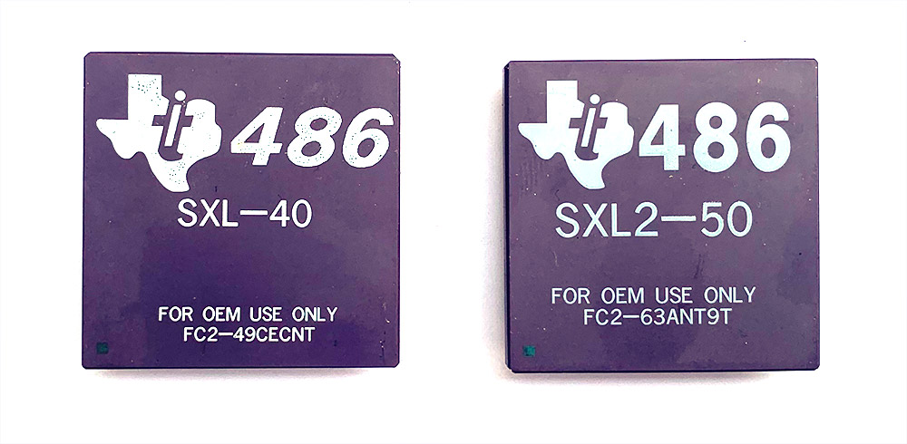
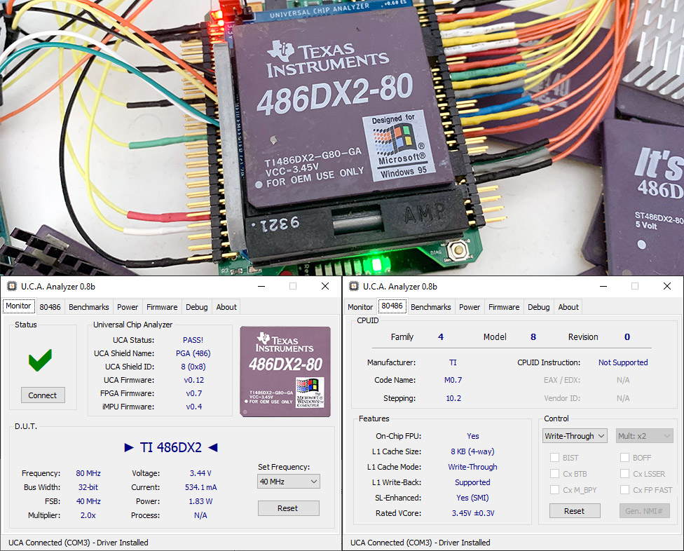
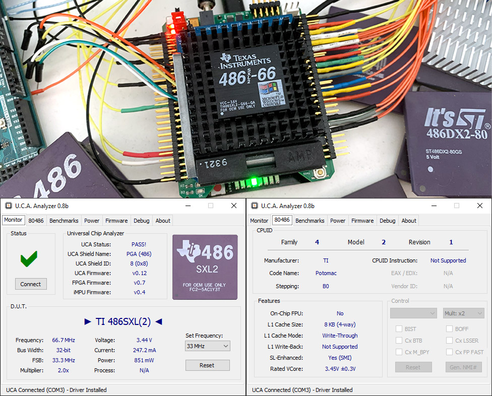
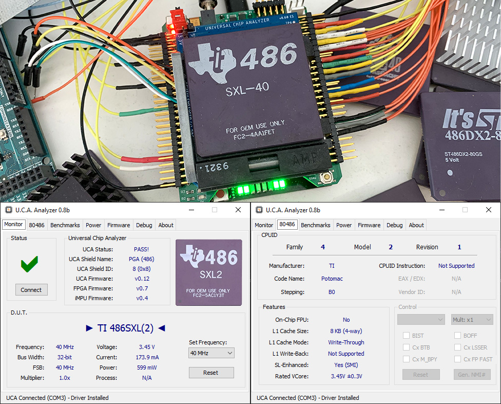
Let’s now talk about the Ti 486SXL. After having simply renamed the Cyrix 486DLC to Ti 486DLC, Texas Instruments released a new, reworked core they called the “486SXL”. It was available with PGA132 (386) and PGA168 (486) pinouts. Two models were released for PGA132 Socket: the TI 486 SXL40 and the TI 486 SXL2-50. Here they are:
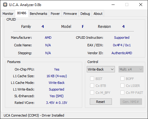
 They come with two major differences compared to the Cyrix 486DLC. First, TI boosted the L1 cache from 1 KB to 8 KB (same size as the Intel 486). Then, the clock-doubling feature (also available on the SXL-40 despite its name) is not always activated by default like on the DRx². It must be enabled after boot by software. You basically have to mess with internal proprietary registers to enable the clock doubling mode.
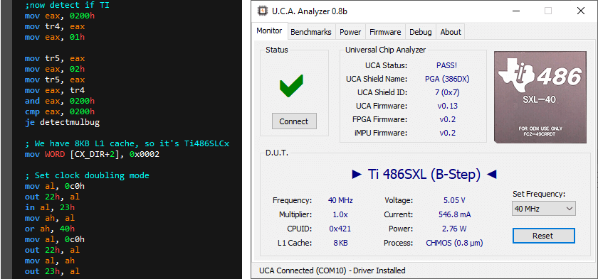
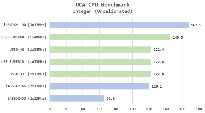
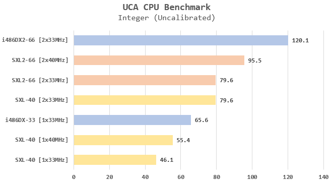
Very few 386 motherboards support the Ti 486SXL but the UCA happily tested it with and without clock-doubling. Just for fun, I ran some benchmarks on all 386s now supported by the Universal Chip Analyzer. The code is not really well-tuned and is only based on some register manipulations and a lot of math integer operations (add, sub, imult and idiv). Here are the results:
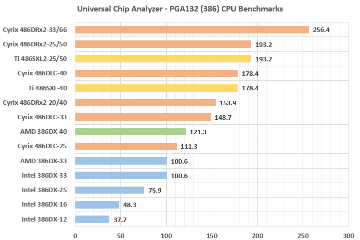
Intel 386s appear as the slowest of them all. AMD 386s performances are exactly the same as expected but their famous 40 MHz model offers a 20% boost versus the Intel 386 DX-33. Cyrix 486DLC are much faster. When introduced, they claimed “up to 2x faster than 386DX at same clock frequency”. Our test showed a ~50% improvement between the Intel 386DX-33 and the Cyrix 486DLC-33. The 486DLC-40 is ~80% faster than the fastest Intel 386.
Anyway, the most impressive performance come from the DRx²: the rare 33/66 MHz version is actually ~7x faster than the original Intel 386 DX released at 12.5 MHz in 1986! Results from the TI486SXL show it’s entirely based on the Cyrix 486DLC core with no tuning at all on the microarchitecture. The effect of the increased 8 KB cache is invisible because the UCA has an extremely fast RAM without any wait-states (similar to the L1 cache). Anyway, even real-world applications don’t benefit from a big gain (no more than 3-5% at best).
Stay tuned for more exciting news from the UCA!

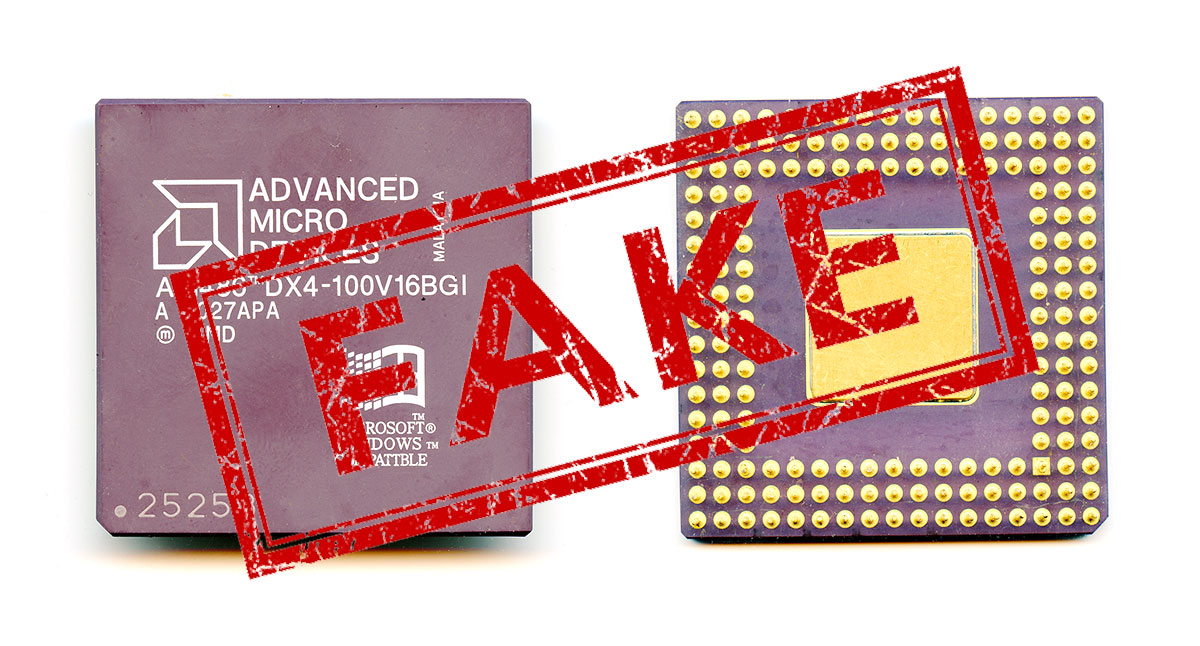
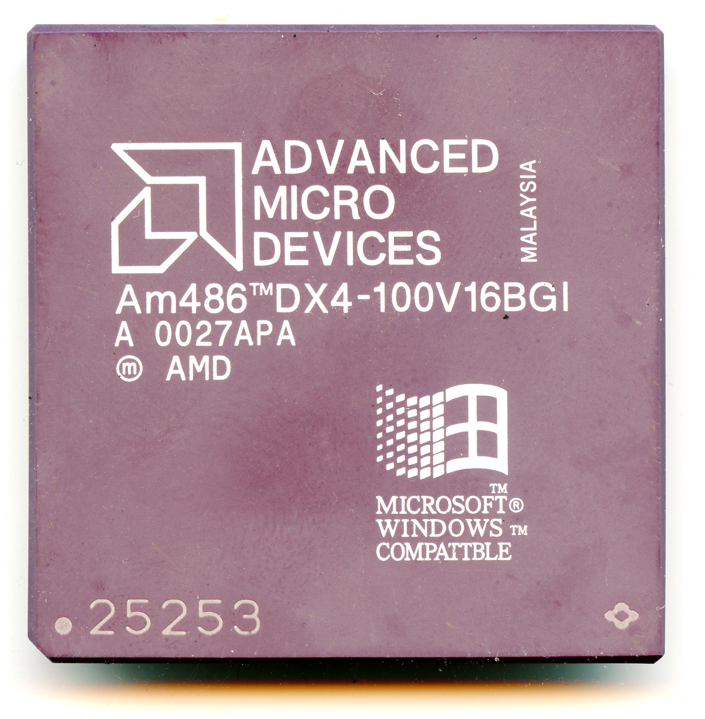
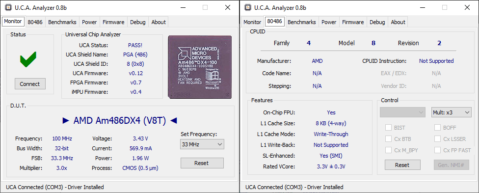
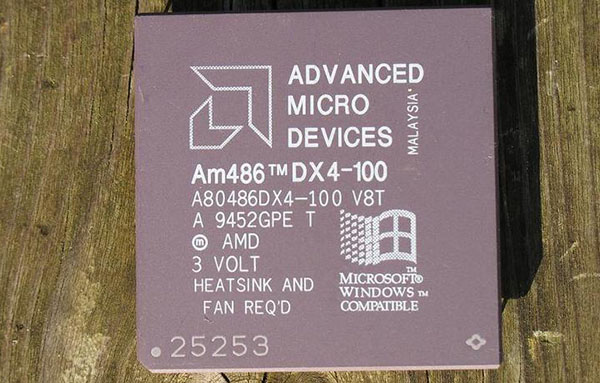
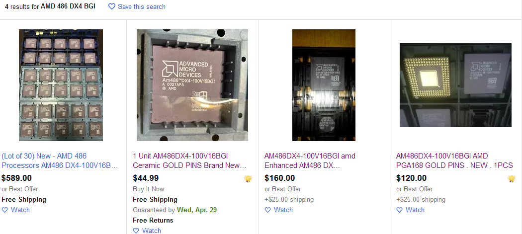
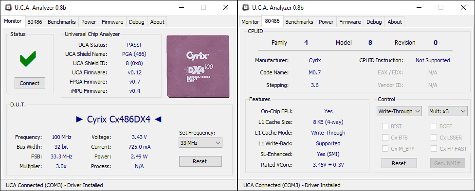
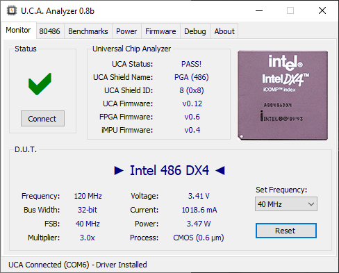
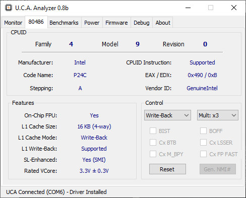
 There is no doubt at this point that this CPU is a counterfeit Am486DX4. The only question remaining is when was it remarked by fakers? Counterfeits CPUs – especially 486s – were common in the 90s to boost frequency, but here, the original CPU was already an Am486DX4-100 (albeit a very early one with 8 KB L1 Write-Though Cache, instead of the expected 16 KB L1 Write-Back Cache). More recently, in the mid-2010s, old CPUs from the 90s were also faked to target CPU collectors all over the world.