Counterfeits CPU were very common in the mid-90s. The worst period was between 1993 (just after the launch of the Intel 486 DX2) and 1998 (when the Pentium II started to be multiplier-locked). It was extremely easy for tricksters to remove the original marking and reprint another one with a higher frequency rating. Many DX4-75 were remarked to DX4-100, and even more Pentium 133/150 were remarked as Pentium 166 or 200s.
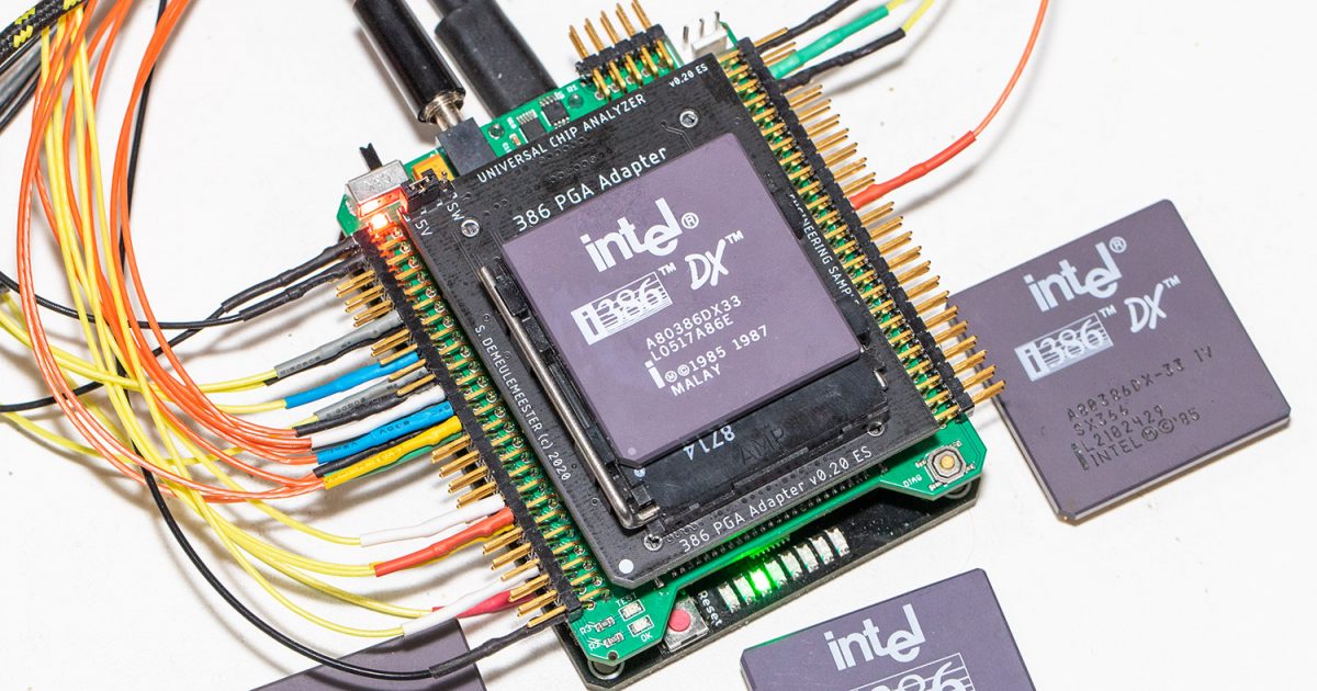
Genuine factory-remarked CPUs also exist, but they’re generally uncommon. The most well-known example is the double-sigma (ΣΣ) sign added on early 386s after they had been tested bug-free from the infamous 32-bit multiplier bug. Some rare Intel 486 SX were also later remarked with a higher speed grade. Here are two of them:
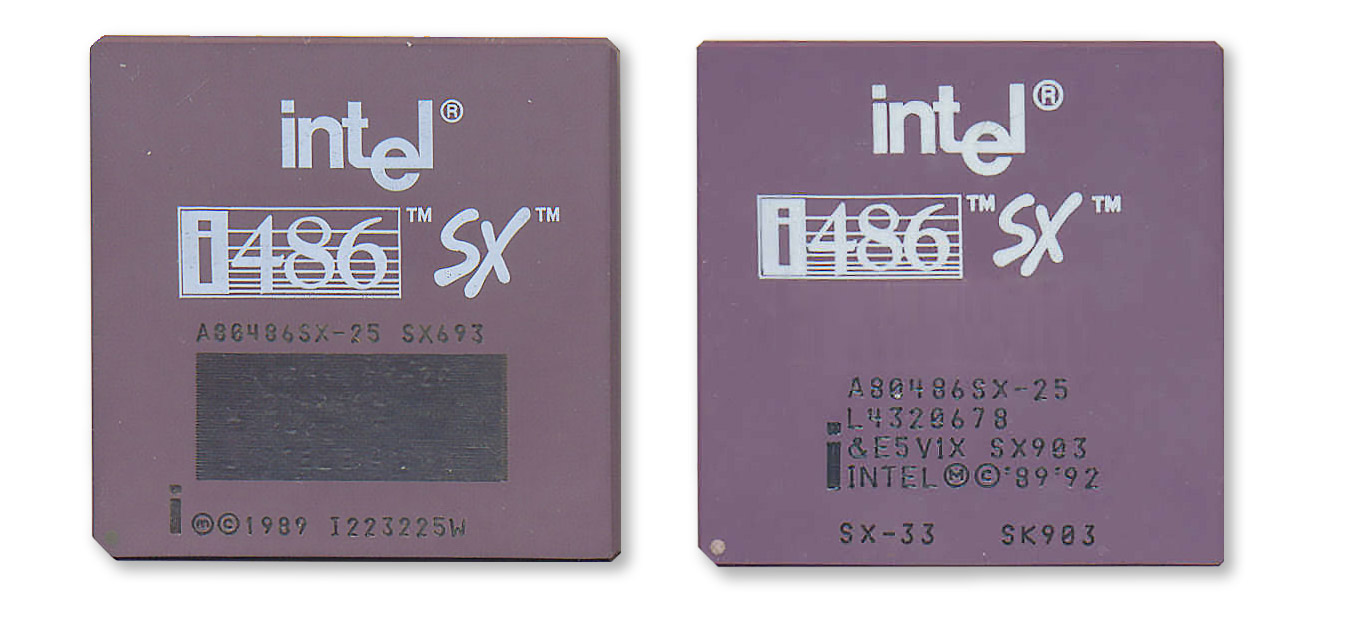 As for all factory-remarks, the addition is quite obvious. Intel probably binned twice these CPUs again at the request of a big customer (IBM?) and added the second rating later. Today’s story about factory-remarks is much more unusual because it concerns standard models.
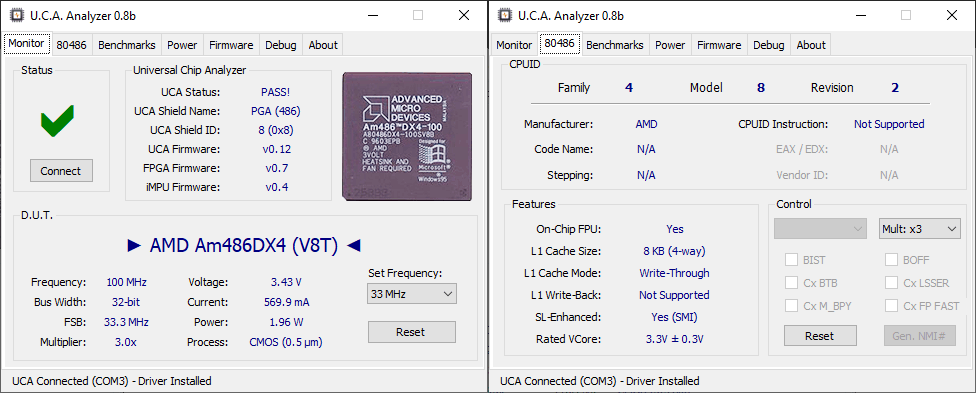
Am486DX4-100SV8B (remarked 5×86)
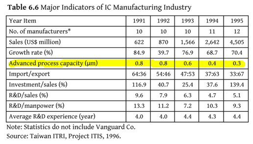
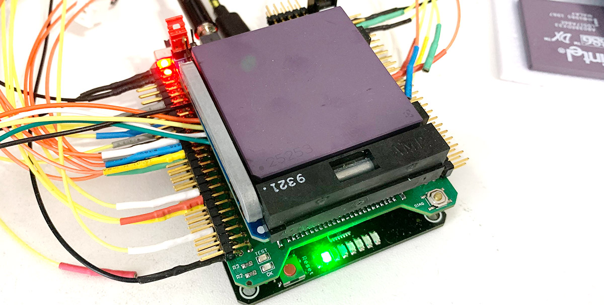
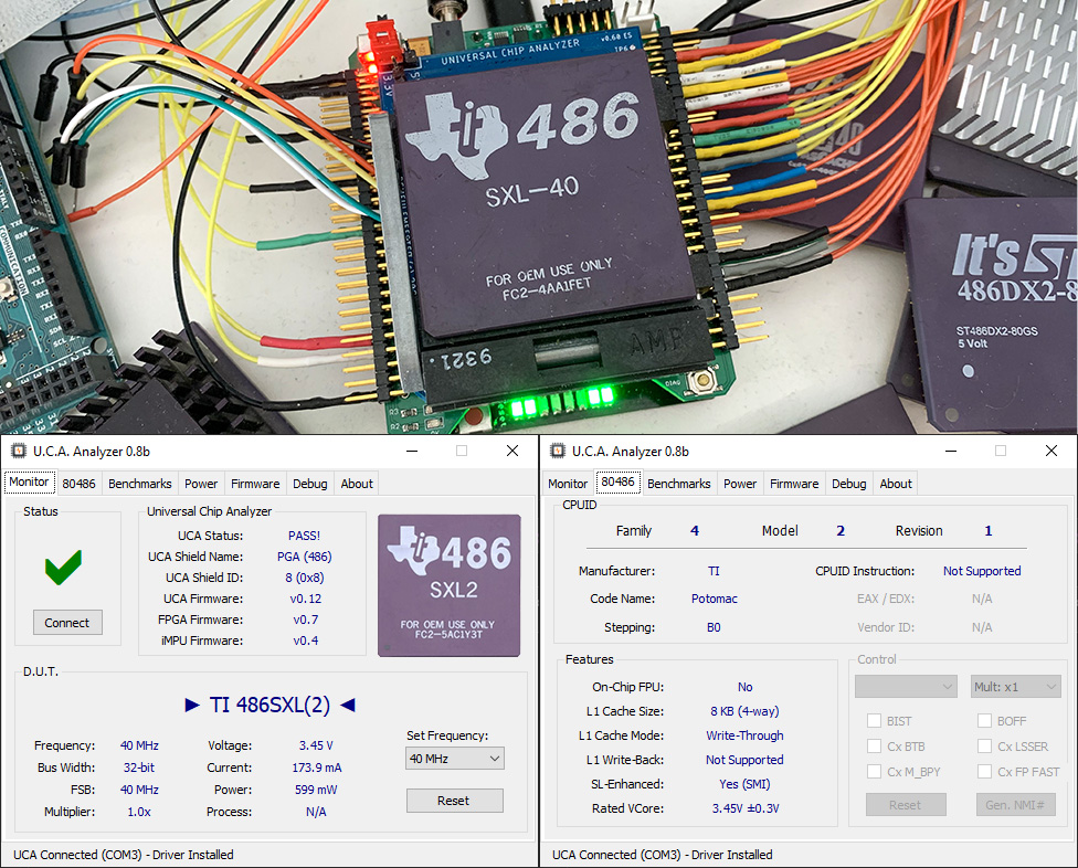
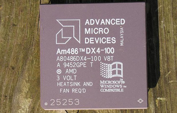
After I published this analysis some weeks ago, a reader told me he had a strange Am486DX4-100 that seemed to be a AMD 5×86. After a careful look at the printings that looked 100% genuine at first sight, he was kind enough to lend it to me for further investigation with the UCA. Here it is:
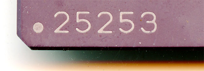
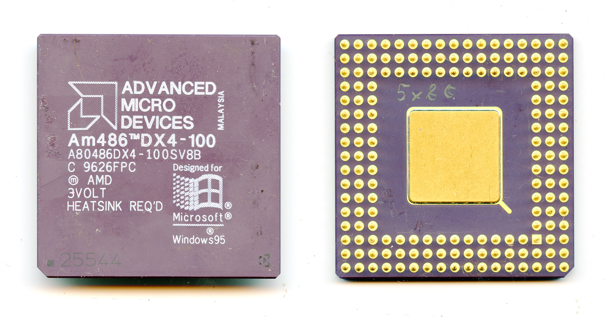 The “9626” date code tells us it was manufactured in late June or early July 1996, which is quite late for a Am486DX4. I immediately noticed the 25544 package code, only used for the 350 nm die. This die was the basis of all Am486DX5 and Am5x86. The “C” stepping was also unusual as the Am5x86 is based on the A-step (from November 1995) or B-Step (from March 1997). A “C” Stepping build in 1996 is incoherent with the 5×86 line, but very coherent with the 486DX4 (later 486DX4 in the latest “C” Stepping were built on the 25498 package in May/June 1996). So it was time for a test on the Universal Chip Analyzer:
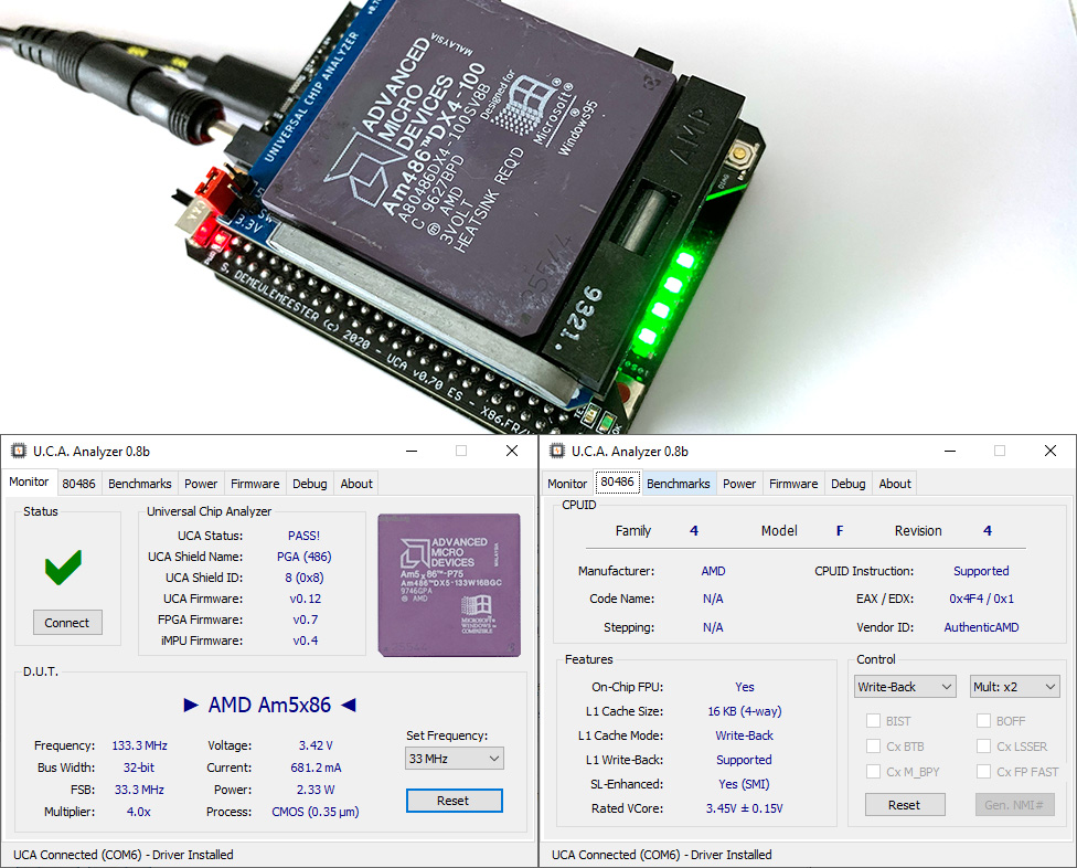
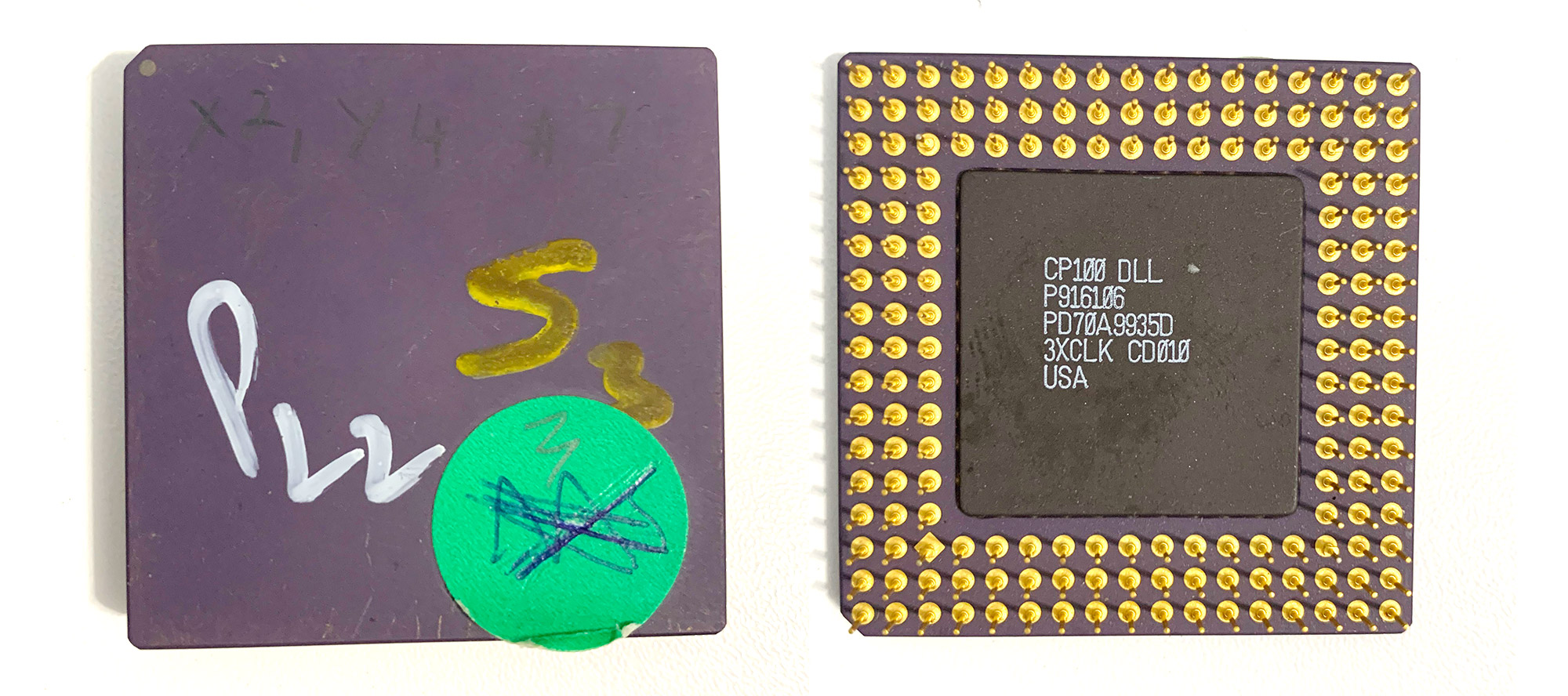
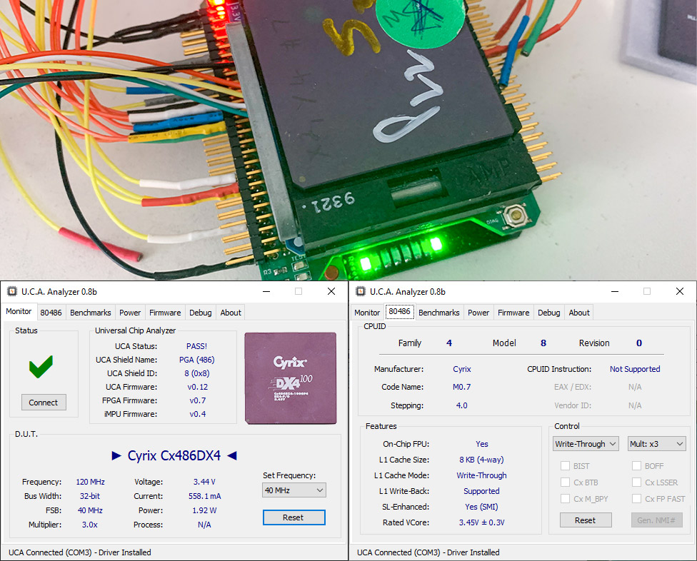
WOW! There is no doubt: this CPU is really based on the standard 350 nm die with a fully enabled 16 KB Write-Back L1 cache and a working 4x multiplier. Actually, it can even be overclocked easily to 133 MHz. All specs, including power consumption and CPUID (0x4F4), make it indistinguishable from an AMD 5×86. This CPU can of course also work with a 3x multiplier like an AMD 486DX4-100 (CPUID drops to 0x494).
After some research, it seems that all CPUs based on the 25544/C package are marked as 486DX4-100SV8B while being really DX5 SV16B (5×86). AMD produced them for quite some time between February 1996 and March 1997. They probably stopped the production of the old 500 nm die in early ’96 but still had some demand from customers for DX4s, so they just used the new 350 nm die and marked these CPUs as DX4-100s. As long as you use the default x3 multiplier, they behave exactly like the old one … except for the cache size.
Has Intel also done such weird things? I could have sworn no way. I was wrong…
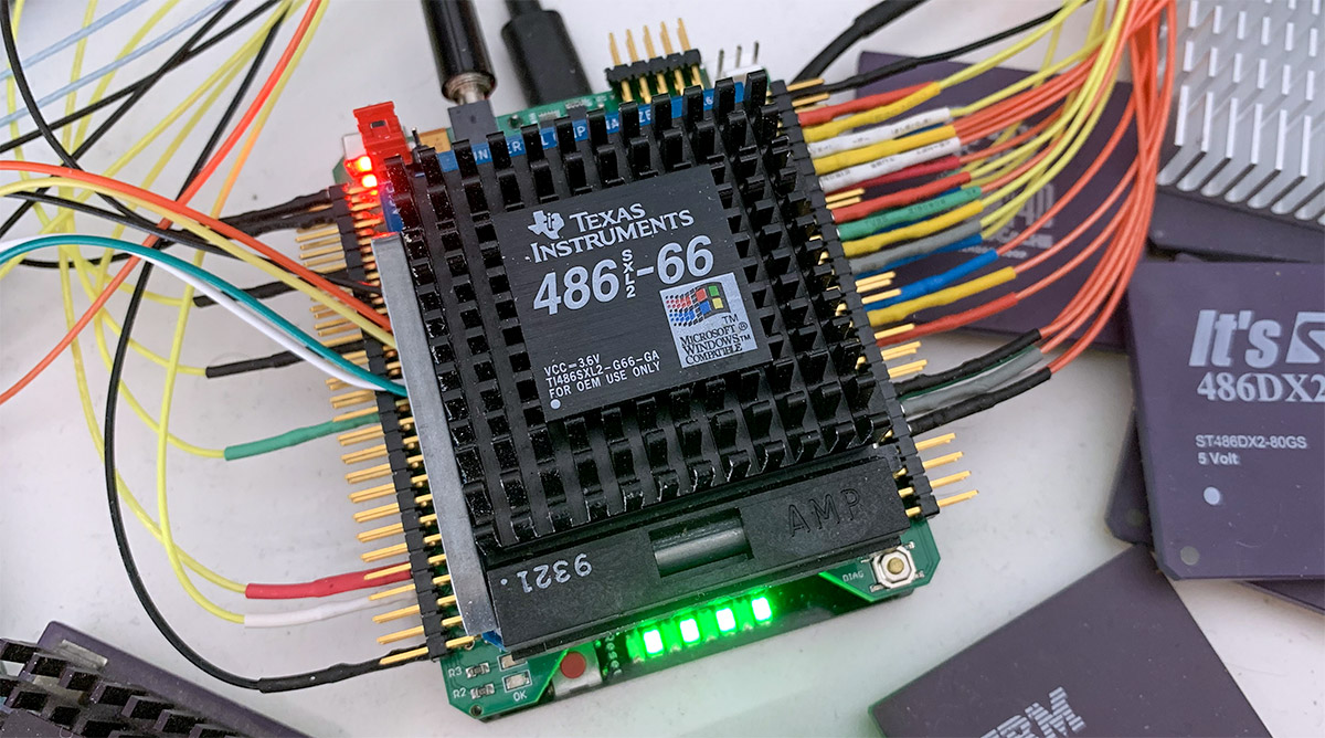
Intel 486DX2-66 SK080 (remarked DX4)
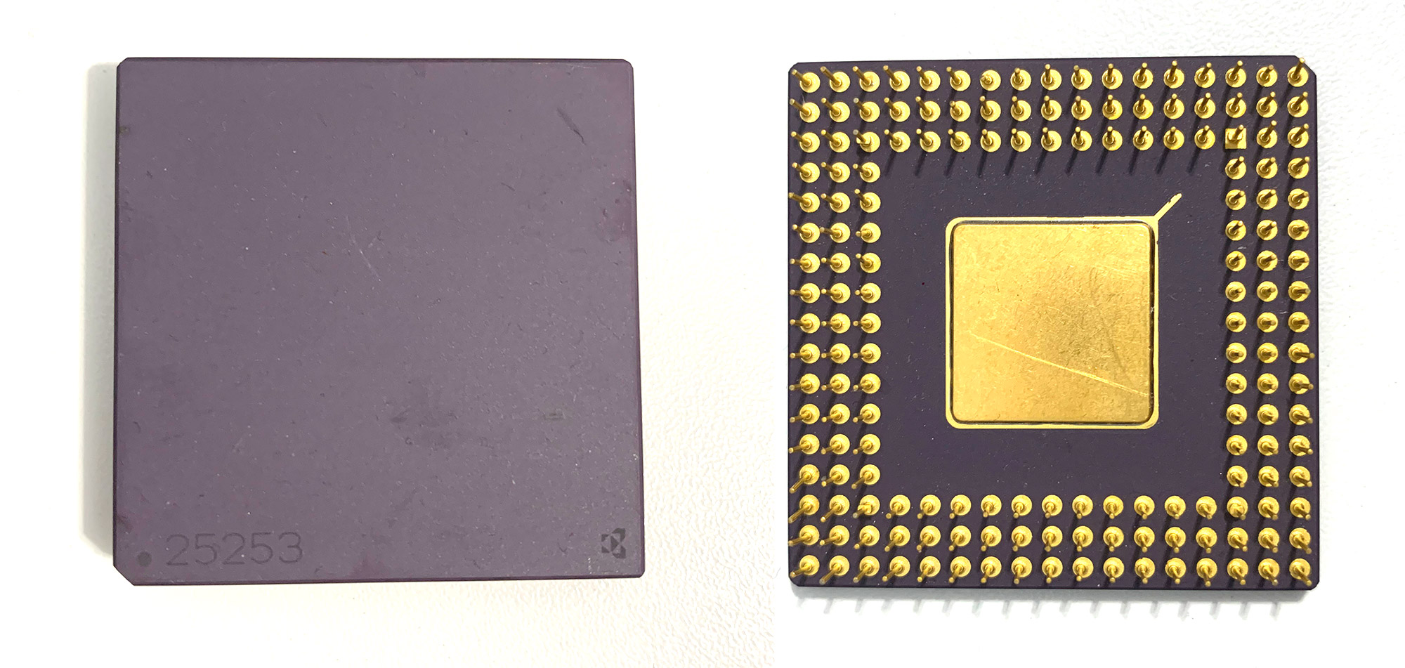
The same reader also sends me a DX2-66 that could be “really a DX4-100”. That sounded odd and really unlikely to me because Intel has a strict policy on S-Spec. Intel DX4s also have a specific CPUID to help distinguish them from DX2s by software. Unlike AMD 486s, this CPUID does NOT change with the multiplier used, so it’s strange to have a DX2 with a DX4’s CPUID. Here is the original CPU:
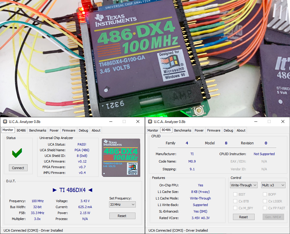
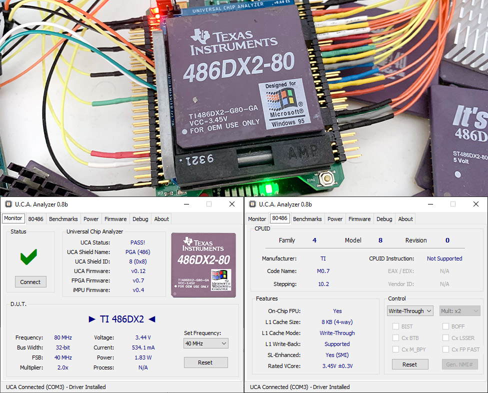
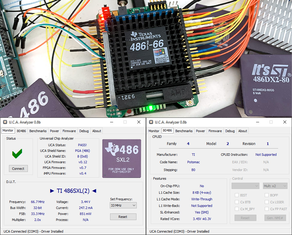
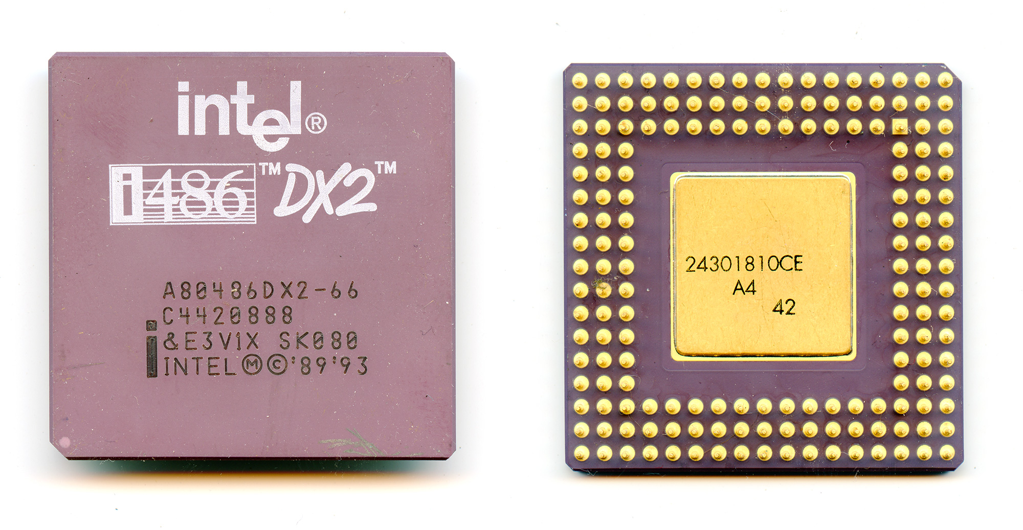 Everything looks genuine here. SK080 is one of the least common S-Spec for Intel DX2s. The only other S-Spec beginning with “SK” is the extremely rare SK058. The SK080 is a 3.3V SL-Enhanced part which seems to have been produced only between WW18’94 (May 1994) and WW48’94 (November 1994). Let’s plug in into the UCA:
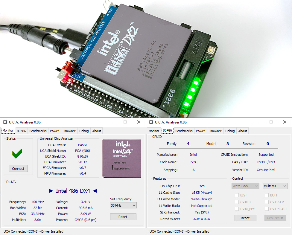
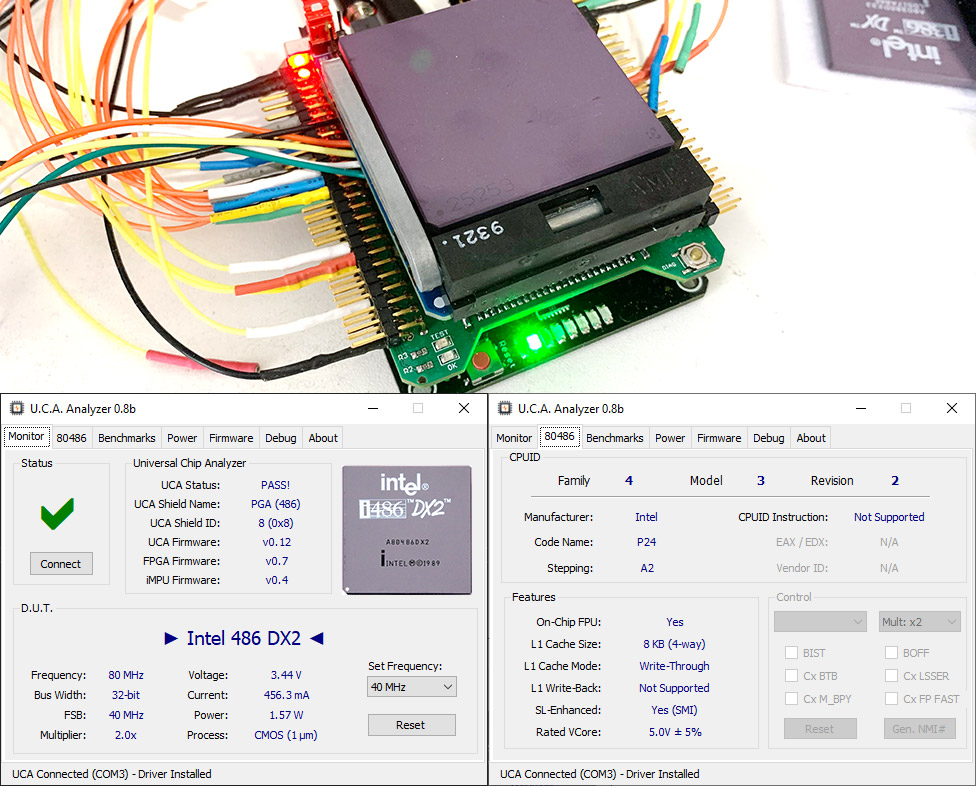
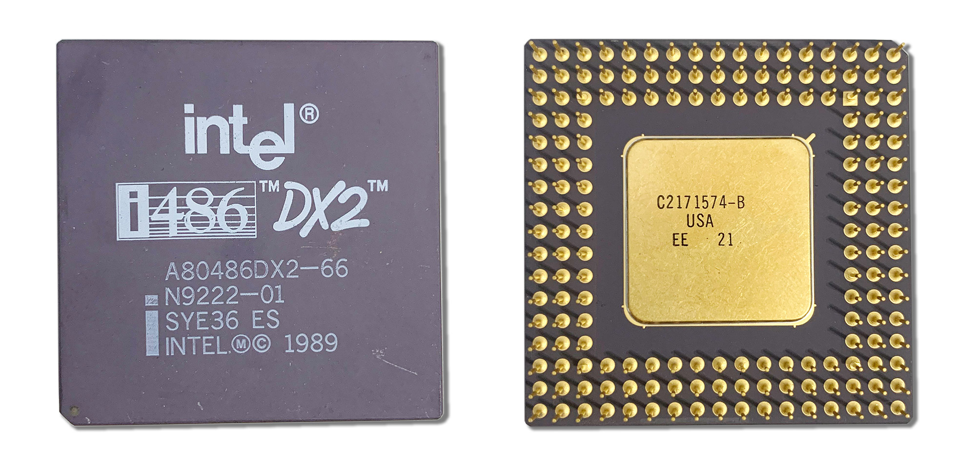
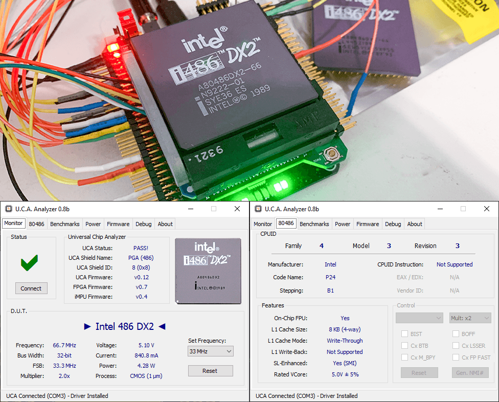
Awesome! This is really a DX4 factory-downgraded to DX2-66. The 0x480 CPUID leaves no doubt about the original die used here. The usual power consumption and the ability to work fine at 3.3V at 100 MHz let me think it’s probably a DX4-100. With the multiplier set at 2x, the SK080 also works at 2×33 MHz as expected for a CPU marked as a DX2-66. To be 100% sure, I was able to find another sample to confirm these findings.

![[Guide] Am486 Die & Packaging](https://x86.fr/wp-content/uploads/2020/07/allpackages-1200x622.jpg)
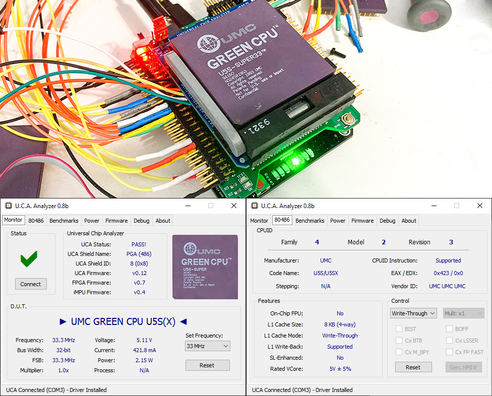
![[UCA CPU Analysis] Prototype UMC Green CPU U5S-SUPER33](https://x86.fr/wp-content/uploads/2020/05/banner-2.jpg)

![[UCA CPU Analysis] Intel 486 DX2-66 SYE36 ES](https://x86.fr/wp-content/uploads/2020/05/banner.jpg)
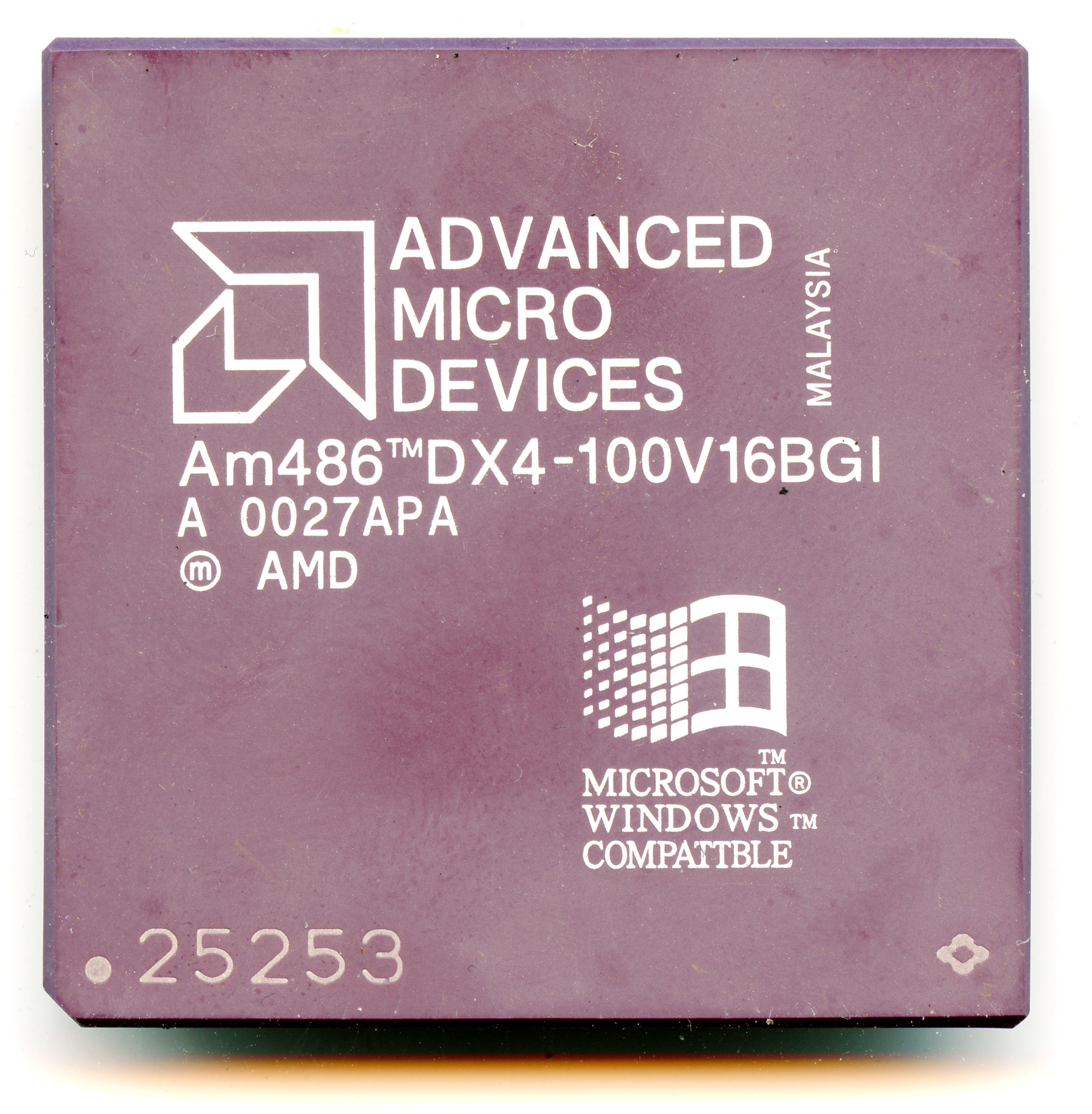
 There is no doubt at this point that this CPU is a counterfeit Am486DX4. The only question remaining is when was it remarked by fakers? Counterfeits CPUs – especially 486s – were common in the 90s to boost frequency, but here, the original CPU was already an Am486DX4-100 (albeit a very early one with 8 KB L1 Write-Though Cache, instead of the expected 16 KB L1 Write-Back Cache). More recently, in the mid-2010s, old CPUs from the 90s were also faked to target CPU collectors all over the world.