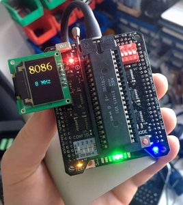
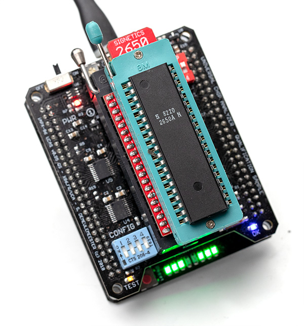
The U.C.A. now supports Motorola 6800!

Finally, two years after a Intel 8088 (almost) booted for the first time on a very early UCA, I’m glad to announce the support for the last major 8-bit CPU : the famous Motorola 6800 !

The Motorola 6800, released in 1974, was one of the most advanced CPU in the 70s. Being TTL-compatible and only requiring 5V power, it was also  easy to use for hobbyist (albeit a two-phase clock was mandatory). Unfortunately, its high price prevented the 6800 to reach the DIY “mainstream” market. Many computer pioneer preferred the MOS 6500 and the Intel 8080, but Motorola  soon released a much cheaper, MCU-revision of the 6800 – the 6809 – that has been very successful.

The architecture of the 6800 is quite simple but efficient. It uses two accumulators, a 8-bit bidirectional data bus, a 16-bit stack pointer, and a 16-bit dedicated address bus that could address 64 KB of memory. Unlike the Intel 8080, the Motorola 6800 uses memory-mapped I/O : it doesn’t include specific instructions for I/O and they are handled as standard memory accesses.

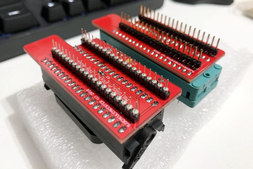
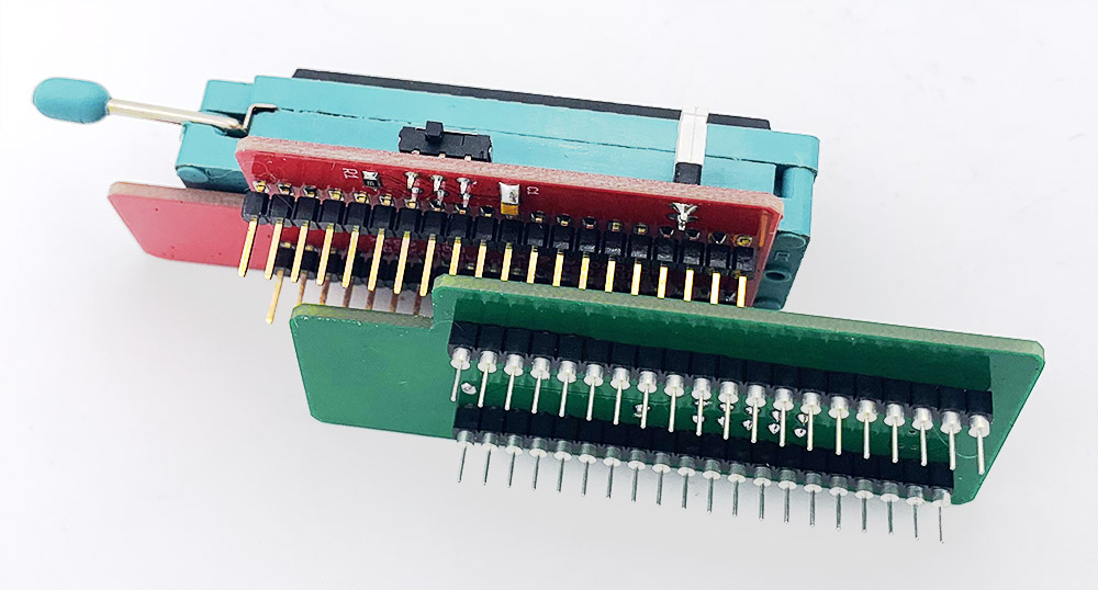
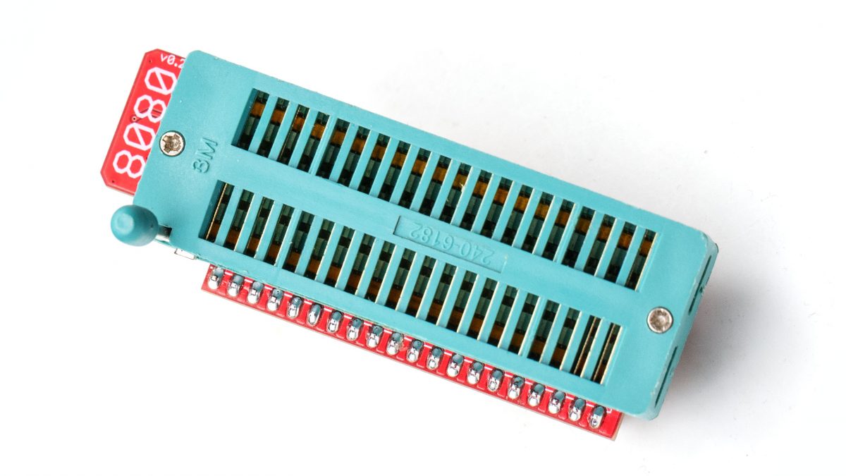
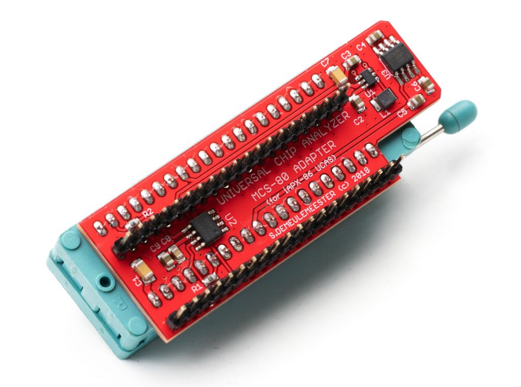
Implementing support for the 6800 on the Universal Chip Analyzer (U.C.A.) wasn’t too difficult. The dual-phase clock was the main issue, as timings are usually tighter than with single-phase clock. Another issue was the UCA adapter. I designed it to support both MOS 65xx and Motorola 68xx, but the cheap chinese ZIF Socket (3M clone) I soldered on was crappy. The contact between the adapter and the main ZIF Socket wasn’t also very good, due to the standard 2.54mm pin header. Too thick, too square. So I build another adapter with a much more efficient Socket (an ARIES low-profile, burn-in ZIF Socket) and some new pin headers that mimic a real CPU :

The new Socket with “real” CPU pins (front) VS the old one (back)

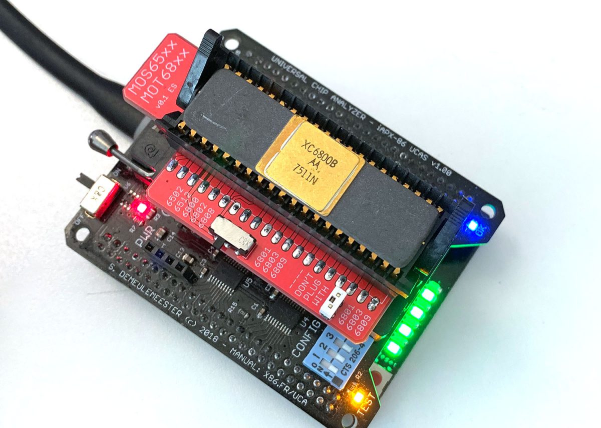
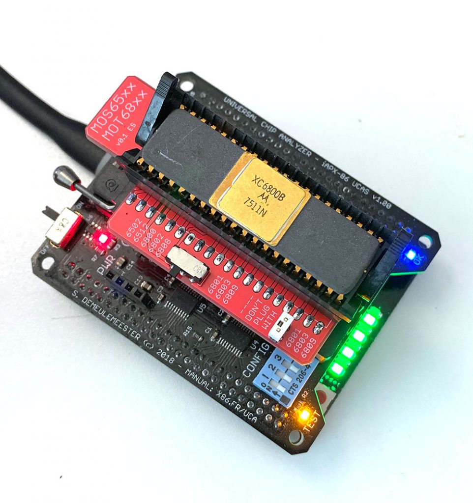
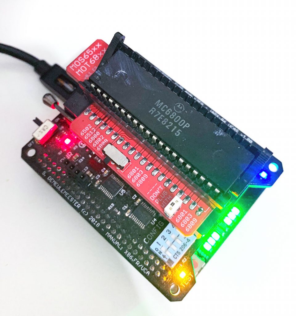
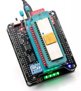
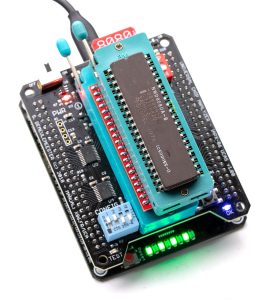
Everything worked as expected and very reliably with that new adapter! Here is the UCA testing a Motorola MC6800P at 2 MHz and a very rare prototype (Motorola XC6800B) at 1 MHz :

Testing frequency can be set at 1.0 / 1.5 / 2.0 or 3.0 MHz to match the most popular 68xx.

Support for Motorola 6801/6802/6803/6808/6809 is planned soon.

More important, a brand new era is coming for the UCA, as I can now focus on much more advanced, 32-bit CPU. Many news planned soon!

U.C.A. Test & Calibration Adapter

Not really some big deal here, but I wanted to share some new “internal” tools I developed for the Universal Chip Analyzer. I ship them quite slowly due to long PCB assembly process, but the final testing process was also quite time-consuming. I used to test all U.C.A. with every supported CPU and, if something goes wrong, I inspected every IC and connector to find the issue.

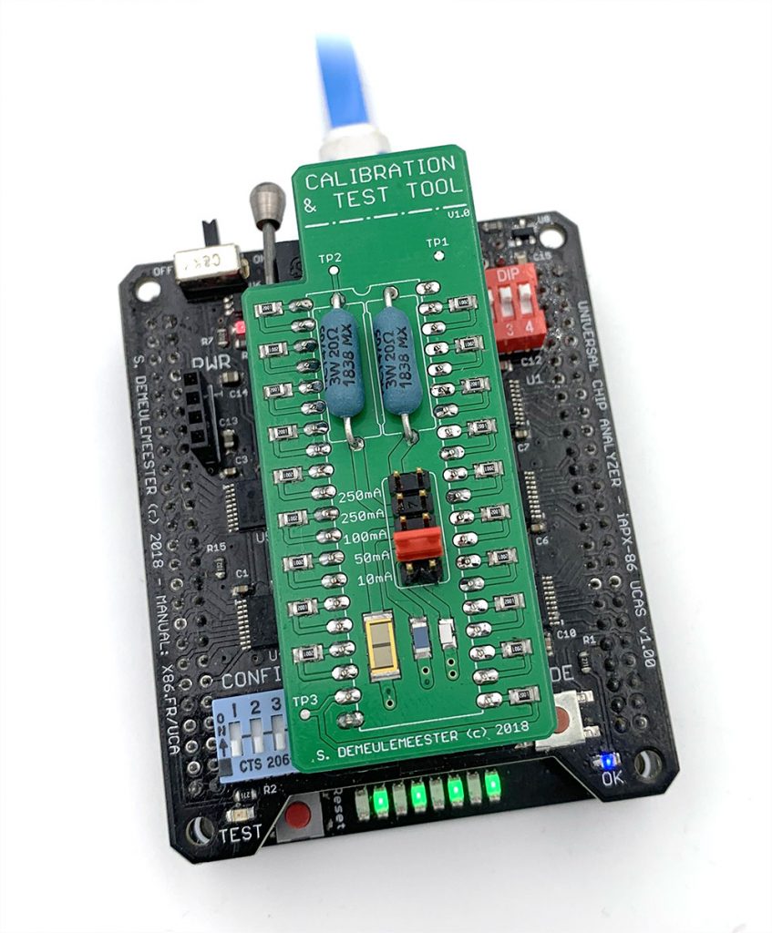
I was a bit tired so I build that “calibration & test adapter” :

With a special test program loaded inside the FPGA, I’m now able to test every pins for stuck-to-0, stuck-to-1 and shorts in seconds! I have also added precision resistors to calibrate the internal shunt amplifier & ADC. Calibration data are now stored inside the internal EEPROM (and saved locally for any UCA serial#).

I’m also testing a new kind of “header” for Adapter’s pins. Previously, I used standard 2.54mm headers. They worked fine in most case, but the pins are much thicker than standard CPU’s pins. I was able to find these connectors that almost perfectly mimic CPUs pins :

They’re not cheap, but I will probably use them for active adapters like the 8080 Adapter.

Stay tuned for much more news soon!

The U.C.A. now supports MOS 6502!

Since the end of last year, I faced a lot of change in my personal life: new job, new house, new car, etc. Except my girlfriend, almost everything else changed in the last 3 months. Damn exciting, but I had very little time to spend on side projects.

It’s now time to resume the work on the Universal Chip Analyzer! My next goal was to add support for the very successful MOS 6502, an 8-bit microprocessor released in mid-70s that was at the heart of many designs well into the 80s.  The original 6501 (circa 1975) was pin-compatible with the M6800 while being much less expensive, but Motorola sued MOS almost instantly and the 6501 has been withdrawn very quickly. The 6502 shares the same internal micro-architecture with the original 6501 but uses a different pin arrangement.  It’s a very simple CPU, with a 8-bit accumulator, two index registers and a 16-bit address bus (able to interface with a maximum of 64 KB of memory). The 6502, just like many other early CPU, doesn’t have a specific way to handle I/O: you must define an arbitrary memory-mapped I/O range and configure your hardware accordingly.

Several variants of the MOS 6502 has been launched through the decade, some of the them with reduced addressable memory (6503 to 6507) and some others with additional features (6508 to 6510, …). Many early computers and consoles are based on a 6502: Apple IIe, Commodore 64, Atari 2600, Nintendo NES, Oric Atmos, etc.

Adding support for the 6502 wasn’t as easy as I expected. The main issue came from the timings. Usually, I drive all the logic inside the FPGA with the the clock signal generated locally and sent to the CPU. That doesn’t work with this particular CPU because it integrates an internal two-phase clock generator used to sync external IC. So, I finally had to feed these two clocks back in the FPGA and sync the internal logic with them. Some delays were needed to match the original timings (FPGAs hate delays) but everything now seems to work properly.

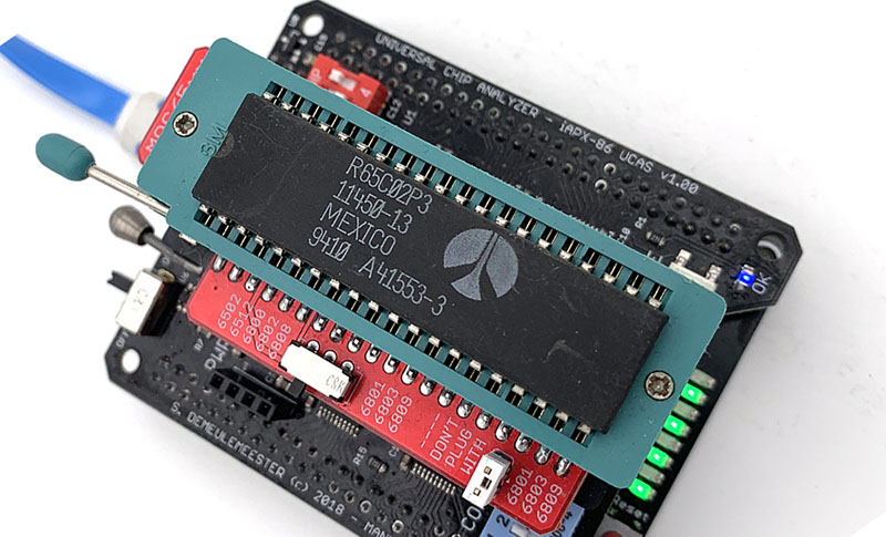
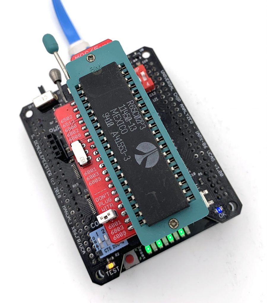
Here is the UCA testing a NMOS Rockwell R6502P at 1 MHz and a much more modern CMOS Rockwell R65C02 at 4 MHz (overclocked from 3 MHz):

Testing frequency can be set at 1.0 / 2.0 / 3.0 or 4.0 MHz to match the most popular 65xx

I’m waiting to get some samples to support other 6502-based CPU like 6510 or 28-pin 6503 -> 6507. A Rockwell 65C112 has already been seen working properly. The passive adapter isn’t final now, because I still need to work on my next goal: the Motorola 6800! This CPU Is the last (but not least) big one I need to support with the UCA. Stay tuned!

The U.C.A. now supports Intel 8080 !

A new milestone for the Universal Chip Analyzer (U.C.A.) : it now supports Intel 8080s, one of the very early CPU released by Intel in 1974! I originally planned to create a complete UCAS (UCA Shield) to support the 8080, but I was finally able to design a small UCA Adapter for the iAPX86 UCAS.

This is the first “active” UCA adapter (both the adapters for Zilog Z80 & Signetics 2650 are only passive). The biggest issue with the 8080 was the power requirements : unlike all CPU supported so far by the UCA, the 8080 doesn’t work with a single +5V supply rail. It also needs +12V & -5v. +12V has been created from +5V with a TI DC-DC Boost Converter and -5V is generated using a charge-pump IC.

Some signals like the two-phase clock are also not TTL compatibles and requires a true MOS voltage swing (0-12V). For the first alpha prototype, I tried some high-speed transistors as voltage translators, but I wasn’t able to meet the tight rise/fall time (~25 ns) expected by the 8080. I then tried a Dual MOSFET driver and it worked perfectly. All components are packed on a tiny adapter the size of the previous passive ones.

Testing frequency can be set at 2.0/2.6/3.1 or 4 MHz

Intel 8080A

Intel D8080A-2 ES

The expected “retail” price for the 8080 UCAS Adapter is ~$25.

Stay tuned for the next big announcement!

UCA progress & Xeon ID UCAS (Early prototype)

Some news about progress done on the Universal Chip Analyzer :

  • About the UCA itself (modded Mojo v3 board), I found a reliable source for assembled board and they will be modified soon. All firmware features are now implemented and working correctly. UCA FW v1.00 is close.
  • About the iAPX86 UCAS, a first batch has been ordered from Elecrow, but they soldered a wrong component on them (well, 50+ wrong components). So I had to send back the whole batch to China. Unfortunately, the package now seems frozen somewhere in China! Tracking is EW001348809FR if you want to check… If it get lost, I will lose $400 and I’ll have to order another batch. Sad.
  • Anyway, when I got the package from Elecrow, they added two unsoldered PCBs, so I was able to assemble one of them myself to validate the final 1.00 PCB. Good news: everything is working correctly! Signal integrity is much better than on ES/QS, up to 50 MHz, and all hardware bugs are solved. VERY good news. I tested quickly the new expansion port (dedicated for future uses) and it also works as expected.
  • I’m working on a new UCAS Adapter for the Intel 8080. The goal is to use the iAPX86 Shield to test Intel 8080. They requires +5/+12 & -5V, so the Adapter will be an active adapter, but the 8080 is TTL compatible. The design is done and proto PCB will be ordered soon.
  • I’m also working on 3 different UCA Shield :
    • The MOS/MOT UCAS for Motorola 68xx & MOS 65xx CPUs. There is no real technical difficulties on this one from the tech side.
    • The MCS-4/-40 UCAS for Intel 4004 & 4040. LOT of technical challenge here. Interfacing a 45+ years old PMOS CPU that requires -10V/+5V with a modern 3.3V FPGA is quite hard. Especially while using ONLY modern ICs. I’m still working on the schematics right now, messing with comparators, zeners and transistors. The HDL code will not be easy, but I have some ideas.
    • A new “Universal PGA Shield” (UPGA). I finally decided to cancel the iAPX-286 Shield that I already showed working on early stages. Why? Because having a 286 UCAS, a 386 UCAS, then a 486 UCAS and another 486 3.3V UCAS, and another 68000/68010/68020/etc. UCAS will be  expensive. The UPGA UCAS will support all of them at once, with (quite cheap) interchangeable Sockets. The design have been done, focusing on the fastest 486DX/DX2/DX4.  If my design works for them (not proven right now), it will also works with all slower CPUs like 386 or 286. Schematics are done and a nice 4-layer PCB has been designed. It’s a very complex PCB, so I don’t expect the Rev 0.10 to work without massive rework. Fingers crossed!

Now, let me introduce another concept for the UCA : the Xeon ID UCAS! I have big plans for the Universal Chip Analyzer as a truly “Universal” chip analyzer, and this is one of them. Xeons are sometimes hard to identify, especially Engineering Sample (ES are often unmarked, available in various flavor with the same part number, or unknown in databases). Xeon motherboard are also a nightmare to work with, expecting exotic RAM, 2- or 4- CPUs, with BIOS restricted to a few S-Spec. Fortunately, “True” Xeon  – like MPs but not the rebranded Desktop CPUs – comes with an embedded “PIROM” chip, used by the motherboard to check their specs without booting the whole CPU. The “Xeon ID UCAS” uses that PIROM to ID the unknown Xeon.

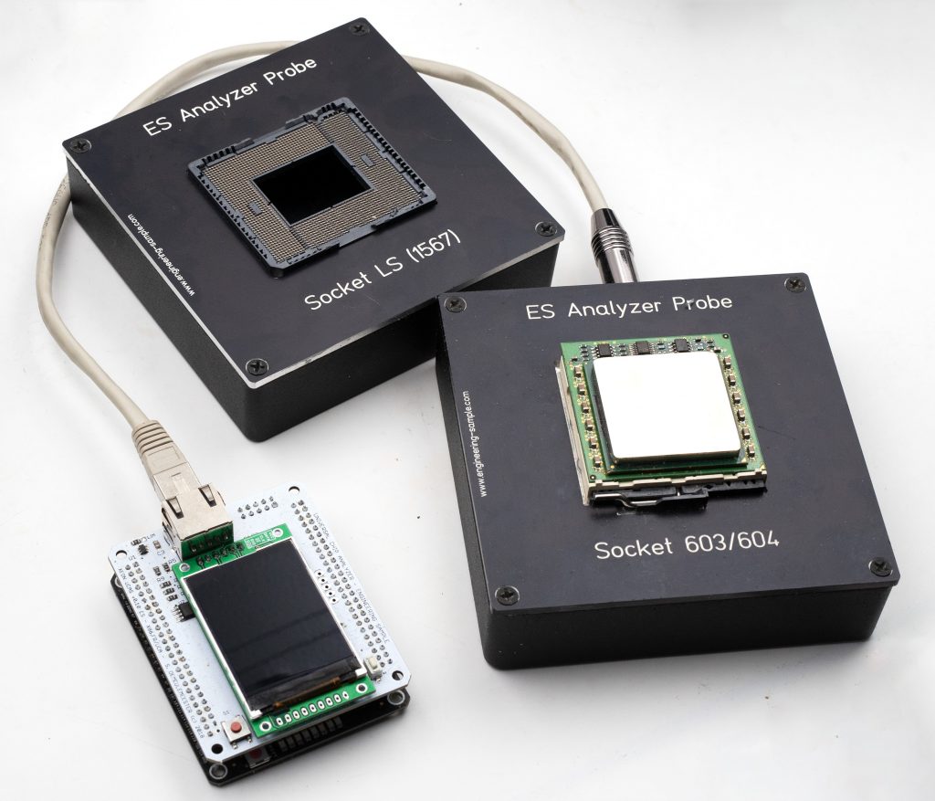
The Shield interfaces with Socket probes to connect with the CPU. Right now, I have a working Socket 603/604 Probe and a LGA1567 Probe, but the UCAS should also work with Pentium II/III Xeon (Slot 2) and up to modern Xeon (LGA2011/3467).

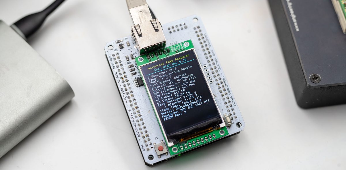
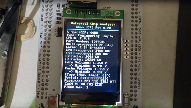
Many information can be grabbed that way. Here is an example with a quite-old Xeon (Gallatin) QF75 ES  :

And here with a later Xeon (Tulsa) QQBB ES (Intel Xeon 7140M) :

lightboxI also made a small video to let you see how it works:

That’s only a proof-of-concept right now, and the Socket Probe will not be cheap if ever sold, but it looks quite nice 🙂

Stay tuned!


The U.C.A. now supports RCA/CDP 1802 “COSMAC” CPUs !

New milestone reached for the UCA !

After days messing with that prehistoric micro-architecture (don’t even have a CALL/RETURN instruction) as well as the VHDL code to implement the tight timings needed, the UCA now supports the RCA CDP1802 (COSMAC) CPU !

Here is a sample of the preliminary test code used

NEXTT: 
    LDI $10         ; LOAD 10h into D
    PLO R4          ; Push D in low byte R4
TEST1: 
    LDI PTRN        ; LOAD byte xxh (the pattern memory location) to D
    PLO R2          ; Push low order byte from D to R2 (=X)
    OUT 1           ; Output the **memory location** at X (=R2) to Port 1 (N0 = 1 / N1-2 = 0)
    NOP
    LDI TLOOP       ; LOAD loop constant to D
    PHI R3          ; Push D in R3's (=X) high order byte
LOOP:  
    DEC R3          ; Decrement R3
    GHI R3          ; Push high order byte from R3 to D
    NOP
    NOP
    BNZ LOOP        ; if D/R3 not zero, loop until zero
    NOP
    LDI PTRN2       ; LOAD byte xxh (the pattern memory location) to D
    PLO R2          ; Push low order byte from D to R2 (=X)
    OUT 1           ; Output the *memory location* at X (=R2) to Port 1 (N0 = 1 / N1-2 = 0)
    NOP
    LDI TLOOP       ; LOAD loop constant to D
    PHI R3          ; Push D in R3's (=X) low order byte
LOOP2: 
    DEC R3          ; Decrement R3
    GHI R3          ; Push high order byte from R3 to D
    NOP
    NOP
    BNZ LOOP2       ; if D/R3 not zero, loop until zero        
    DEC R4          ; decrement R4 (test loops)
    GLO R4          ; put high-byte R4 into D
    BNZ TEST1       ; if R4/D is not zero, loop again, if zero, continue to next test.

Testing can be done at 2.5/3.2/4.0 & 5.0 MHz.

The interesting part is that it doesn’t require any additional adapter, just a firmware update. I designed an adapter for this chip, but it wasn’t finally required.

While developing for the RCA 1802, I found a limitation on the iAPX-86 UCAS’ hardware design : it can’t measure current for this particular IC. The 1802 power consumption is abysmall (< 2 mA) and under the lowest end of the range I choose. The UCAS just can’t reliably measure power-hungry behemoths like the HMOS USSR clones (> 1.5W) and extremely low power chip like the 1802. Not really a big deal..

Anyway, it now works as expected with CDP1802! Right now, I don’t have CDP1804/05/06 but I’ll try to find one of each soon to check if they also works. They should also run fine and I will be able to check their specific features (Internal RAM & extended instruction set).

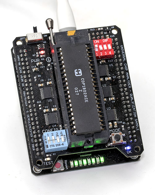
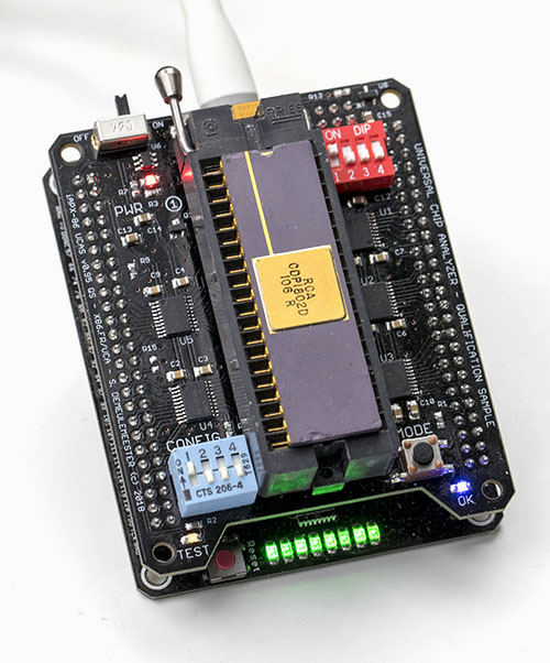
Here are some pictures!

RCA CDP1802D – Tested at 3.2 MHz

Harris CDP1802ACE – Tested at 5.0 MHz

UCA : Advanced Tethered Mode in alpha stage !

Big milestone! The whole communication between all parts of the UCA (from the MCU synthesized inside the FPGA to the USB port connected on the ATMega) is now working as expected !

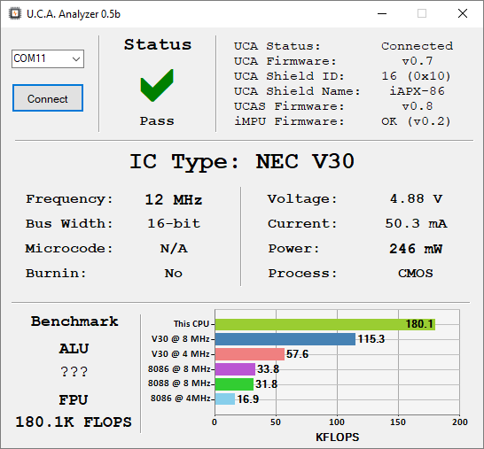
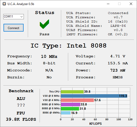
I wrote a simple software in C# this night to show how the advanced features will look like. Top-right, you have the current status of the UCA/UCAS with all the embedded firmware version (yep, there is 3 of them!) . Top-left, the obvious “Connect” Button and the current Status (ranging from “testing” to “Pass” or “Fail” and even “short-circuit”).

In the middle Area, all the feature detected by the UCA : bus width (8088 Vs 8086), Burnin Mode and frequency settings, Microcode (TBD), and also Voltage / Current / Power Drawn by the IC and the corresponding process (CMOS/HMOS/…). I should be able to detect stepping and erratas in hardware for some chips Smile

Finally, in the bottom area, an hardware performance test, 100% handled by the FPGA. Right now, I only wrote the FPU test, but the ALU (Int) test will follow. The absolute value are probably not accurate yet, but the relative KFlops is good. As you can see, the NEC V30 is MUCH faster than a good ol’ 8086 for FPU processing. I will fine tune the benchmark code later, but I’m happy with the progress ^_^

UCA Analyzer in tethered mode testing a Sony CXQ70116P-8 overclocked at 12 MHz

UCA Analyzer in tethered mode testing a P8008-2 overclocked at 10 MHz

The U.C.A. now supports Zilog Z80s

Let’s introduce the first UCAS Adapter.

Some IC families requires a remap of power lines, much harder to implement into the target UCAS then a remap of signal lines. Adding the required hardware to support software power lines remapping on a 40+ pins IC is just too expensive to consider. The solution is a cheap passive adapter (less than $10).

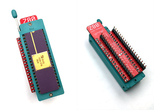
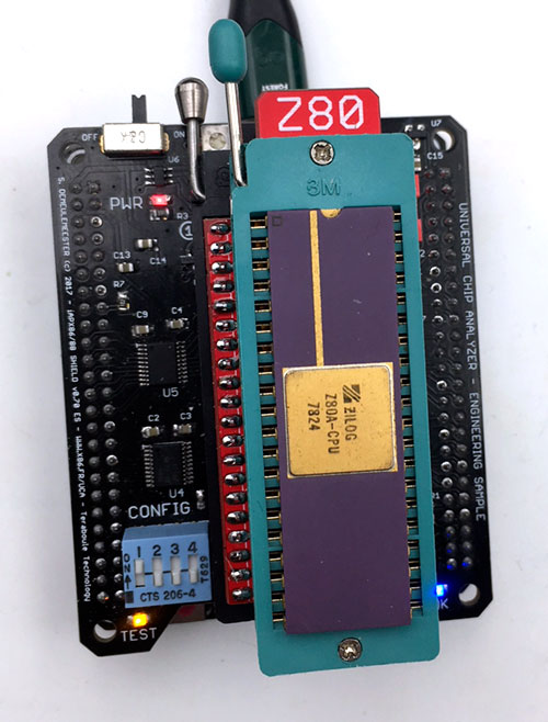
Here is the first one, that add support for Z80 to the iAPX86 UCAS !

Z80 UCAS Adapter
The PCB is cut to allow easy manipulation of the underlying Socket’s lever.

Z80 UCAS Adapter mounted on iAPX86 UCA
A clear indication of the family supported is printed on top.
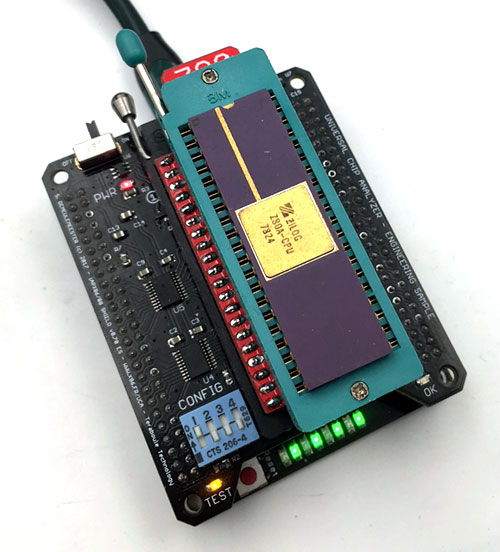
Early Zilog Z80A under testing on Z80 UCAS Adapter @ 4 MHz


The Shield can be configured for 2.5/4/6 or 8 MHz. Tested at 8 MHz with a Z80H and working fine!