I’m so excited to finally disclose my project here for the first time. I know only very people may have any interest in this kind of stuff, but as fellow collectors, you’re certainly in those ones. The idea came to my mind last summer, when I read one of the amazing announcement from molka. I realized that, even if I have some skills in electronics and product design, I don’t have any clues about how earliest CPUs worked back in the 70s & 80s. So, I started to study one of the most successful architecture from that era, the Intel 8086. After some basic experimentation on a breadboard, I then started thinking about an ambitious “universal” IC tester and how to build it.
The Ideal Specs
Ideally, I wanted the specification to be as such:
- Versatile: Able to check the working condition of many different ICs. As much as possible. CPUs, of course, but also other kind of chips like microcontrollers, BSPs, RAMs, and why not FPUs or other support chips. Sounds like crazy because all these ICs are totally different beasts from an electrical interface point of view. Even a 8086 is vastly different from a 8085.
- Advanced: With two testing modes. One basic testing mode, that only requires the UCA and a standard USB power bank to provide the 5V required. You get the result on built-in LEDs. And also one more advanced “analyzer” mode, with the UCA tethered to a computer with USB. With an app, you can get some additional information like real-time power composition, chip identification, working condition, and maybe TBD stuff, depending of the kind of IC tested. On top of that, I also wanted to have “advanced” features. I.e.: testing the working condition of an IC is nice, but testing it at its rated clock frequency is even better. What about overclocking? Benchmark? Could be great too.
- Secure: I’m a CPU collector and I don’t want to burn a costly ES if something goes wrong. The UCA need to be able to detect short-circuit or other defaults. Safety first!
- Compact: I didn’t want a bulky tester. I tried to keep it as small as possible. The actual footprint (8×6 cm) is barely bigger than a credit card.
- Upgradable: Most of the “intelligence” must be in software. The upgradability of the UCA was mandatory. I wanted to be able to upgrade the firmware via USB, to add support for new chips without any (or too much) hardware modifications. More interesting, I also wanted to let the user write his OWN code for the target CPU. So, the UCA can act as a development board.
- Future-proof: When I started my first experiments with the 8088, I had to buy and mess around with Intel 8284 clock generator, bus controllers and other support chips. Some of them aren’t manufactured anymore since decades, are hard-to-find and/or expensive. I wanted to get rid of ANY obsolete chips and I’m only using modern ICs widely available.
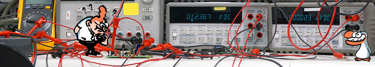
- Affordable: From a technical view, everything I described is close to a device I already own, the Galep-5 Universal EEPROM programmer. It’s a very nice piece of hardware but it costs more than 500€ (and that’s without the numerous expensive adapters often required). I’m not exactly a rich man so I had to keep the price as low as possible. The U.C.A. doesn’t use fancy components. The total BOM is lower than $50. Of course, the final price also depends on manufacturing costs. The fewer I order, the higher the price will be.
So here we are. From all the crazy specs described previously, only a few are working right now. I’m not pretentious enough to tell that all of them will work one day, but the current progress seems to prove the whole project isn’t a total failure. A pretty good start!
How It Is Built
Let’s talk about the UCA. The most obvious central component to use is an FPGA. Microcontrollers are just too slow to interface at full speed with even a 8086 from the 80s, and I have more ambitious target CPU in mind. FPGAs have a lot of IO pins and can be software reconfigurable to accommodate a variety of pinouts. They’re also extremely fast. Main issue (at least for me): developing FPGA and writing HDL code is a nightmare. We’re clearly not in the same world as Arduino or Raspberry Pi.
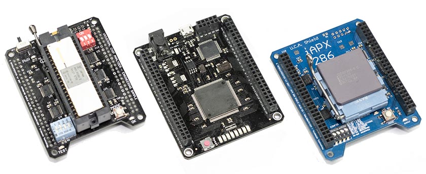
Developing a compact FPGA PCB with 100+ I/O is not extremely complex, but it’s not cheap. You must use a 4-layer PCB (or more) and solder a fine-pitched QFP or BGA IC. In small quantities, the price skyrockets very quickly. So, I looked at the FPGA development boards already available in the market. No need to reinvent the wheel if something suitable was already created and mass-produced. All the UCA’s intelligence is inside the HDL code that emulates (almost) everything and doesn’t require fancy electronics. I found the perfect board: The Mojo from Embedded Micro. It was a successful Kickstarter project launched in 2013 that raised more than $100k.
The Mojo is a simple board packed with an Atmel ATMEGA 32U4 microcontroller, 4 Mb Flash EEPROM and a Xilinx Spartan 6 FPGA. To fit my needs, I modified the original Mojo to add 128 Mb of EEPROM Flash and a stronger voltage regulation. That only requires swapping some components but doesn’t need any PCB modifications, so I was able to keep the original PCB layout. Of course, the original Mojo firmware burnt into the ATMega32U4 had to be rewritten, as well as the original FPGA firmware upload tool.
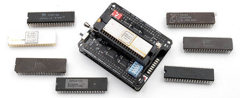
We now have the UCA itself. Then we need an interface to old chips. Modern FPGAs require 3.3V while most IC introduced before mid-90 use 5V (or much higher voltages for the pre-TTL era). The idea here is to use another PCB plugged on top of the UCA (called “UCA Shield” or UCAS). The UCAS is a low-cost, removable PCB. It can be switched to another one to support other IC family. Some UCAS can support many different chips, just by setting a DIP switches. Some chips works without any other modification, just by plugging them into the ZIF Socket, some will require a (very) cheap adapter on top to accommodate different packages (PLCC, LCC, etc.) or different power pinouts.
Current State
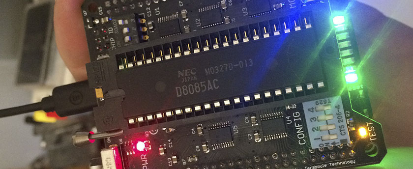
About the UCA, I successfully modified the original Mojo hardware. The firmware has been rewritten to work with the new EEPROM, supports many different FPGA configuration slots (up to 32 right now). I also added many tweaks (automatic detection for shield swap/DIP setting change, A/D converter modification, etc.). The firmware update tool has also been adapted for the UCA. There is still some work required, but the platform is quite stable right now. The whole process of building/uploading/loading FPGA configuration on multiples slot is almost done. Right now, I didn’t start working on the “tethered” part. I added some functions on the UCA firmware, but the Windows part has yet to be done.
About the UCA Shields (UCAS), the whole project started with the iAPX 86 UCAS. The current revision for that Shield is 0.7 and all the most important hardware parts are working as expected. After 3 months of intensive testing, I found some additional tweaks that must be added. Most of them are dedicated to ease the support for some IC. One (maybe two) revisions of the PCB will be required before the “final” one.
Right now, the iAPX 86 UCAS is able to fully test all 8088 and 8086. Clock frequency can be set to 4 MHz (slowest commercially available freq), 8 MHz (8086-2), 10 MHz (8086-1) and 12.5 MHz (overclocking or some Harris parts). 8088s are tested using a 8-bit interface, 8086s with a 16-bit data bus (autodetected). NEC V20/V30 are of course also supported (and detected with the DIAG button). 8018x will require a UCAS Adapter because they use a different Socket. I didn’t start working on this one, but it’s pretty trivial. To validate the concept of complete reconfiguration, I worked on support for 8085 on the iAPX 86 UCAS. All 8085s can now be fully tested just with a different DIP Switch setting. I’m now working on other type of IC (MCS-51, Z80, etc.). Right now, I can’t guarantee any of them will work, but I’m confident they will.
As a proof-of-concept and to demonstrate the power of the FPGA-powered UCA, I also worked on a iAPX 286 UCAS. The revision 0.1 is done and works as expected. It can test any 80286 in PGA/PLCC/LCC. It still lacks almost all advanced features and need a lot of optimization, but it’s only a matter of time. A 386 UCAS is also possible after this one, and perhaps also a 486 UCAS. The main issue is the space required by the ZIF Socket. But I still have a LOT of work before thinking at 386 and newer CPUs…
Some other UCAS are also in the pipe (4004/4040/8008/8080, RAM UCAS, etc.) but I really need to finalize the current shields before starting other ones. That will be a LONG process, probably spread on several years.
Want to Know More?
There is still gazillions of details I would love to share, but I’ve crossed the TL;DR line since a very long time. For the few of you that want to know more, I just started a website describing the project further. It’s far from being finished but you can probably grab some more information there.
UCA website is here: https://x86.fr/uca/
You can see it in action here :
2 thoughts on “Introducing the U.C.A. (Universal Chip Analyzer)”
Comments are closed.