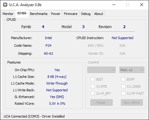
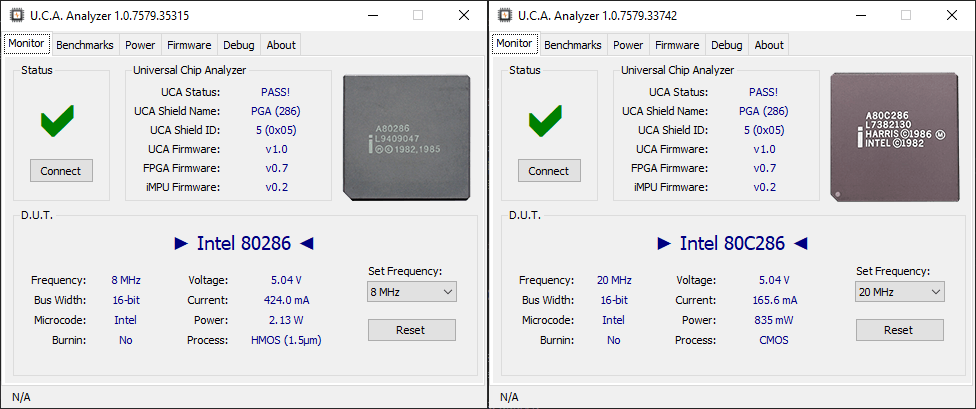
Another milestone – albeit not the hardest one – has been reached! The 80286 is the 2nd gen 16-bit x86 CPU introduced by Intel in 1982. The most important improvement was the use of a separated data and address bus. Its predecessor, the famous Intel 8086, used the same pins to send address and then data. The lack of that slow time-multiplexed bus on the 286 allowed a major performance boost, sometimes more than 100% at a similar clock speed. The microarchitecture also evolved with a more advanced (dedicated) address calculation unit and a faster multiplier. The 80286 was also able to support up to 16 MB of RAM, thanks to its 24-bit address bus.
The 80286 also introduced the protected mode, designed to allow much more advanced memory management, with the ability to build multi-user systems using multitasking applications. Unfortunately, due to several limitations in that first implementation, along with several hardware errata found in earlier stepping, protected mode wasn’t really used by software developers on the 286. Intel only solved all these issues with the 80386. The Intel 80286 was initially released at 4, 6 and 8 MHz on nMOS 1.5 µm process. Later released reached 12.5 MHz in 1 µm CMOS process. Several other companies produced CPU fully based on Intel’s 286 microcode like AMD, Siemens and Harris, with speed up to 25 MHz!
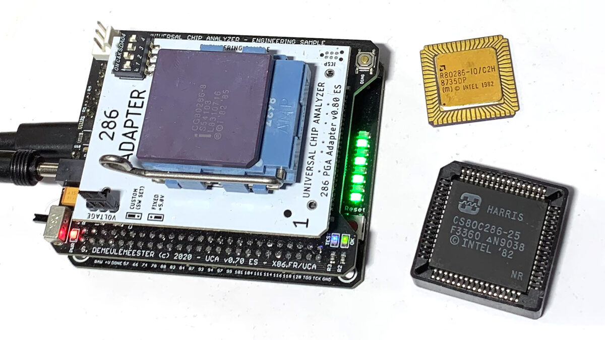
UCA 286 Adapter testing LCC (left) & PLCC (right) 286s
Three common 68-pin packages were used for the vast majority of the 80286s ever produced: the original ceramic PGA, a leadless LCC (also ceramic) and a plastic PLCC. On the picture above, you can see an AMD R80286-8 (LCC) and a Harris CS80C286-25 (PLCC). The Universal Chip Analyzer is able to test all three packages just by plugging the related socket on the PGA DIP Socket. Frequencies available (by DIP Switches or software) are 4, 8, 10, 12.5, 16 and 20 MHz.
Why not 25 MHz? Because the 80286 requires a clock-doubled input and feeding a 50 MHz clock to get the 25 MHz core frequency would have required an external PLL. Not a big deal, but there is only one rare 286-class CPU that supports this frequency (the Harris/Intersil CS80C286-25 pictured above) and its timings is not fully compliant with the 286 specifications. Designing a special UCA adapter just for this chip is trivial, but quite useless because the 286 Adapter is already able to test it at 20 MHz. Speaking about “high” frequencies, using the right socket is crucial
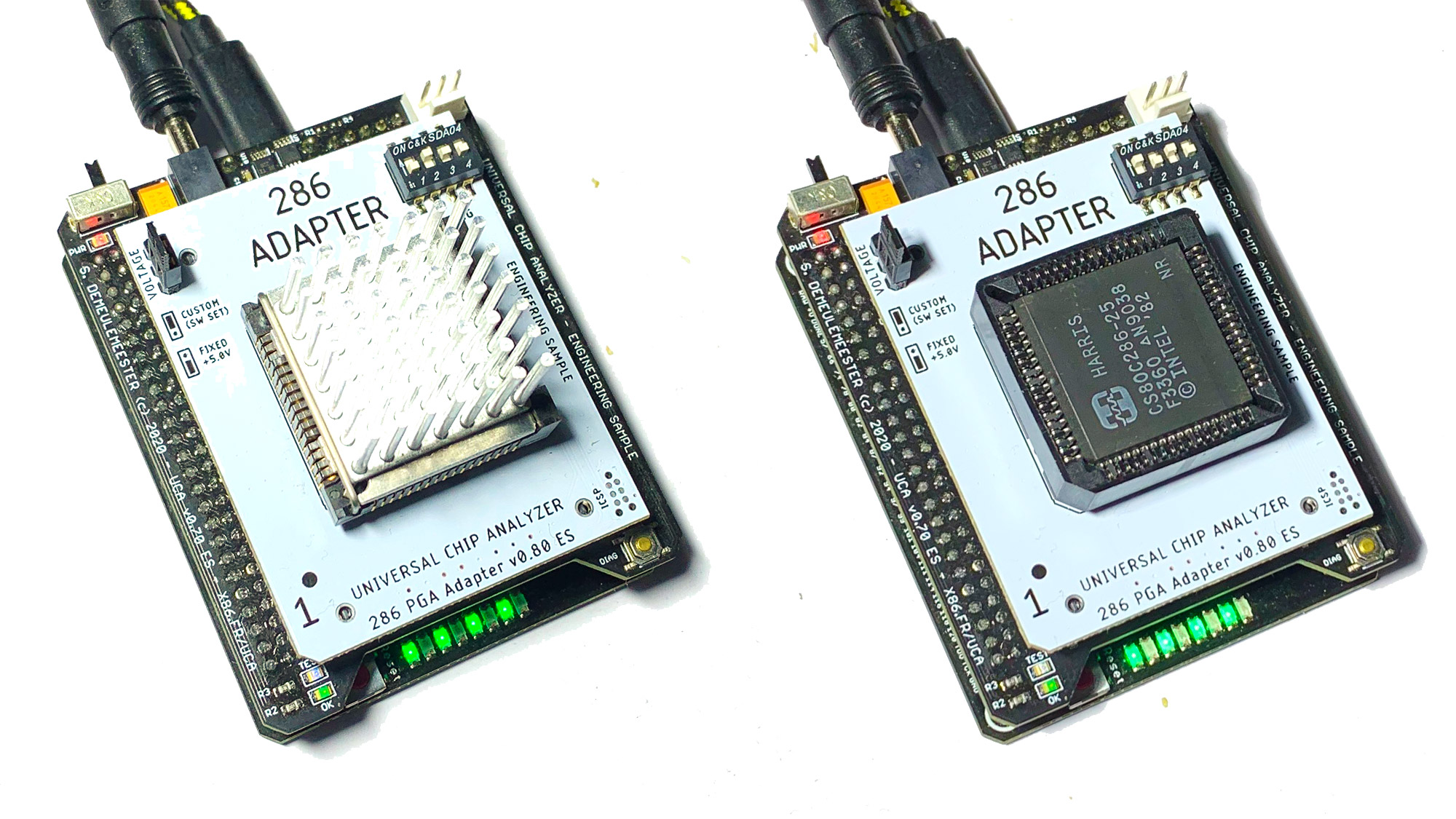
The UCA 286 Adapter is fitted with a high-quality DIP Socket. Directly plugging a PGA 286 CPU is possible but not convenient for testing multiple CPUs in a row. I was able to secure some ZIF Sockets for 68-pin PGA like the blue one pictured here (from AMP) and also some 3M LCC sockets complete with top cap. About PLCCs, I first tried some cheap socket from eBay. That was a disaster: contact pins were too weak and bent after 2-3 insertions. Worst, the maximum frequency allowed was 8-10 MHz. Replacing these crappy sockets with other ones from Foxconn or 3M solved all the issues. I also bought some awesome Yamaichi test Socket for PLCC (on the right), but unfortunately, they use a specific pinout. As the 286 Adapter uses a simple 2-layer PCB, I will consider designing a specific PCB just for them.
With the hardware finished, I’ll later tune the software-testing code to see if I can detect various stepping, and maybe also the manufacturer.
Adding support for Cyrix & TI 486s was supposed to be a matter of hours. It finally took almost one month and gave me many headaches. I almost burned everything to the ground several times in rage, begged for help from FPGA’s gurus who told me what I’m trying to achieve was like squaring the circle, but I did not give up. Let’s try to explain why it was so hard.
— always(@TLDR; Technical stuff) —
FPGAs are synchronous beasts used to create finite states machines: almost everything inside a FPGA is synchronized to a clock signal. Each time the clock is ticking, the HDL code analyzes inputs and sets a pre-defined state (that itself defines registers, outputs, the next state, …). To add support for a CPU, you must read the datasheet and write some HDL code that will provide the correct outputs (from the FPGA to the CPU) within the required timings. All these timings are linked to the base clock. A synchronization between the CPU and the FPGA is crucial. For all other CPUs I’ve worked on for the UCA, the FPGA provides the base clock to the CPU. Both the FPGA and the CPU are sharing the same clock and synchronization is easy. But 386s require a clock-doubled input (80 MHz for a 386DX-40 MHz) that I’m not able to provide directly from the FPGA because the 3.3-to-5 volt translators are too slow. So I use an external clock-doubler PLL, but doing so prevents the FPGA from having access to the CPU clock. That’s the root of all issues I had.
Fortunately, using an external phase-locked loop (PLL) means the clock input phase is synchronized with the clock-doubled output signal: the rising edge of both clocks occurs at the same time. Knowing the transmission delays added by the voltage converters at a given frequency, you can still synchronize your FPGA with the CPU without having access to the base clock. That works fine as long as you don’t change the frequency. But that was too easy: I want to be able to switch frequency on-the-fly and within a large range (from 12.5 MHz to 40 MHz to cover all 386s). That’s still possible if you build many bitfiles (compiled HDL “FPGA firmware”), one for each frequency. Nah! I want to use the same bitfile for everything, including support for both microarchitectures (Cyrix & Intel) despite the different timing’s requirements. That’s hell but I almost succeeded.
The actual firmware is not perfect but I’m quite happy with it because it works as expected in most cases. The remaining issue is a hole between ~21 and ~28 MHz where the FPGA can’t reliably catch the required inputs from the CPU at the rising or falling edge of the clock. My Logic Analyzer is unfortunately too slow to solve this but it’s not a big deal. The HDL code works fine at 12.5 MHz, 16 MHz, 20 MHz, 33 MHz and 40 MHz. The only “retail” frequency I’m not able to do is 25 MHz. I built another bitfile for this frequency only and I’ll hope to find a way to merge everything in the same bitfile later. To avoid losing my mind, I’ll wait to have enough money to buy a faster logic analyzer (like the lovely DSLogic U3Pro32) to work on this again.
— End —
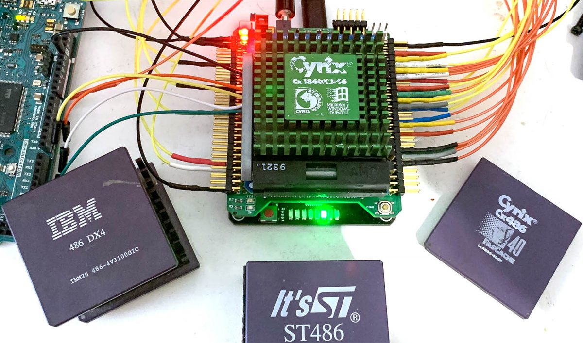
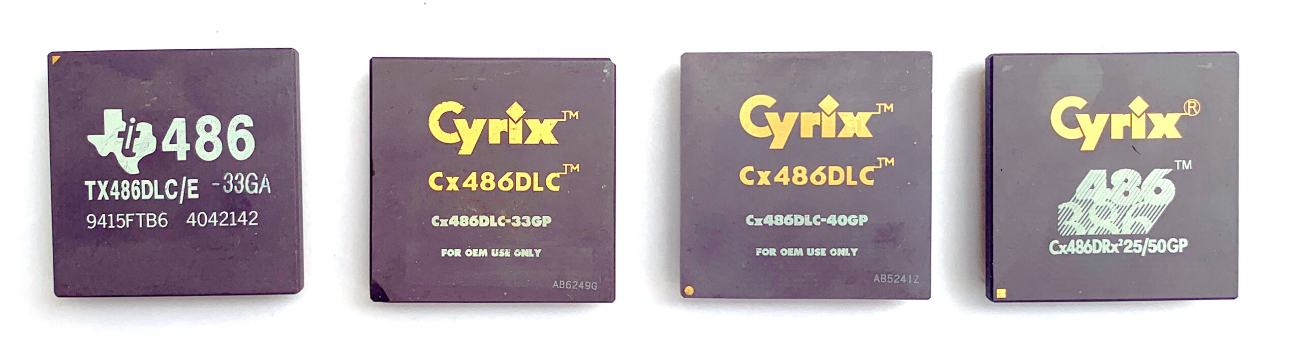
But here it is: the UCA supports all Cyrix-based 386 like the 486DLC. Here are the ones I used for the test:
Unlike 386-class CPUs from AMD, which are based on Intel’s microcode and are exact clones, the Cx486DLC introduced in June 1992 uses a custom microarchitecture built from scratch by Cyrix. While still using the 32-bit 386 bus, they come with 486-class features like an embedded L1 cache and some new instructions. The Cyrix 486DLC is not a perfect pin-to-pin replacement for Intel 386s as timings are a bit different and cache control lines must be handled by the chipset. Compatibility issues are well known with many – especially older – motherboards. The original 486DLC was available at 25 MHz, 33 MHz and 40 MHz. All of these were manufactured by Texas Instruments on the 0.8µm CHMOS node. Ti also launched their own, rebranded 486DLC chips, which were exactly the same except for the marking. Please notice the vicious 90° rotation between printings and pin 1 on the Ti486DLC. Fortunately, the Universal Chip Analyzer have strong short-circuit protection built-in…
Cyrix also later released a special, clock-doubled version called the 486DRx². It was available at 16/32, 20/40 MHz, 25/50 MHz and even 33/66 MHz. This later one was the fastest PGA132 CPU ever released.
Cyrix 486DLC-40 & Cyrix 486DRx²-25/50 Tested on the UCA
The original Cyrix 486DLC exists with two steppings: the earliest one with CPUID 0x420 and a later one with CPUID 0x421. The proprietary “DIR” identification registers available on Cyrix’s CPU is only available on newer CPUs. None of the 486DLC tested have them. The 486DRx² is the only one to have DIR registers and reports itself as Model = 0x07. The UCA happily tested the 486DLC at 40 MHz and was even able to overclock my 486DRx2 25/50 at 33/66 MHz for a short time. Cyrix 486s run hot and deserve a proper heatsink. Power consumption is as high as a 486 DX2 and can go as high as 4 watts (4 times higher than a later Intel 386 DX-33)!
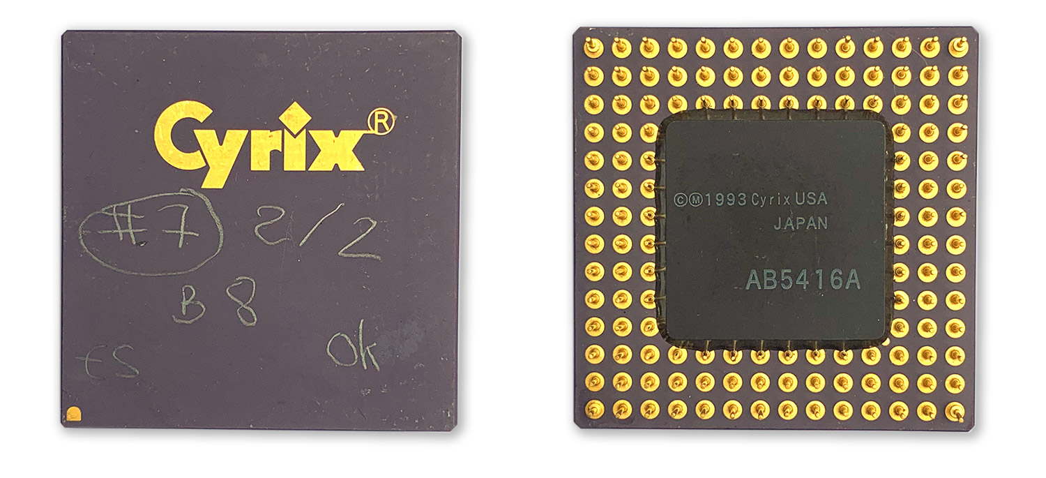
Much later in the development process, I feel confident enough to try a blank 486DLC Engineering sample I got many years ago.
This ES is not a clock-doubled CPU like the DRx² and was able to run properly at 33 MHz. CPUID is 0x421 and – surprise! – it has DIR registers, identifying itself at Model = 0x01 (the expected value for a Cyrix 486DLC) and stepping 0x22, with seems to match the handwritten value (2/2) marked on top. The DRx2 25/50 tested above comes with stepping 0x21, so this ES seems newer. I don’t know at this point if any 486DLCs were released commercially with this stepping – or even if any retail 486DLCs have DIR registers enabled.
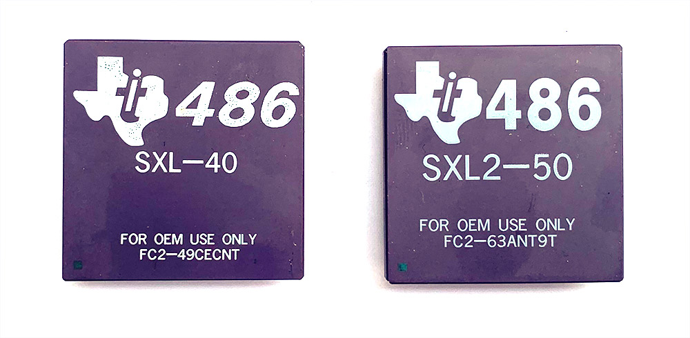
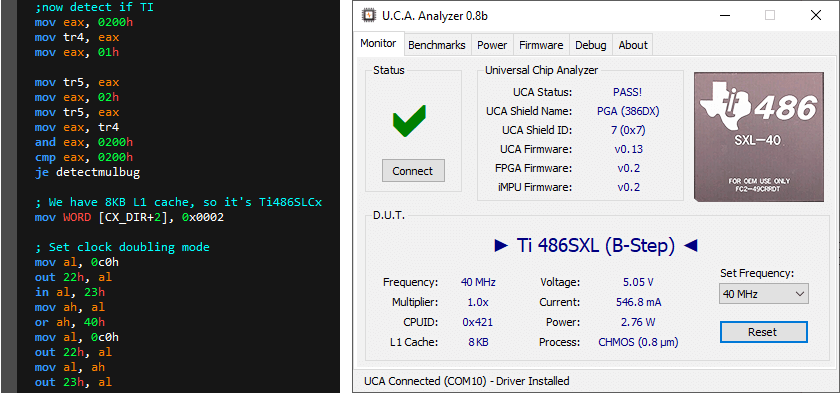
Let’s now talk about the Ti 486SXL. After having simply renamed the Cyrix 486DLC to Ti 486DLC, Texas Instruments released a new, reworked core they called the “486SXL”. It was available with PGA132 (386) and PGA168 (486) pinouts. Two models were released for PGA132 Socket: the TI 486 SXL40 and the TI 486 SXL2-50. Here they are:
They come with two major differences compared to the Cyrix 486DLC. First, TI boosted the L1 cache from 1 KB to 8 KB (same size as the Intel 486). Then, the clock-doubling feature (also available on the SXL-40 despite its name) is not always activated by default like on the DRx². It must be enabled after boot by software. You basically have to mess with internal proprietary registers to enable the clock doubling mode.
Very few 386 motherboards support the Ti 486SXL but the UCA happily tested it with and without clock-doubling. Just for fun, I ran some benchmarks on all 386s now supported by the Universal Chip Analyzer. The code is not really well-tuned and is only based on some register manipulations and a lot of math integer operations (add, sub, imult and idiv). Here are the results:
Intel 386s appear as the slowest of them all. AMD 386s performances are exactly the same as expected but their famous 40 MHz model offers a 20% boost versus the Intel 386 DX-33. Cyrix 486DLC are much faster. When introduced, they claimed “up to 2x faster than 386DX at same clock frequency”. Our test showed a ~50% improvement between the Intel 386DX-33 and the Cyrix 486DLC-33. The 486DLC-40 is ~80% faster than the fastest Intel 386.
Anyway, the most impressive performance come from the DRx²: the rare 33/66 MHz version is actually ~7x faster than the original Intel 386 DX released at 12.5 MHz in 1986! Results from the TI486SXL show it’s entirely based on the Cyrix 486DLC core with no tuning at all on the microarchitecture. The effect of the increased 8 KB cache is invisible because the UCA has an extremely fast RAM without any wait-states (similar to the L1 cache). Anyway, even real-world applications don’t benefit from a big gain (no more than 3-5% at best).
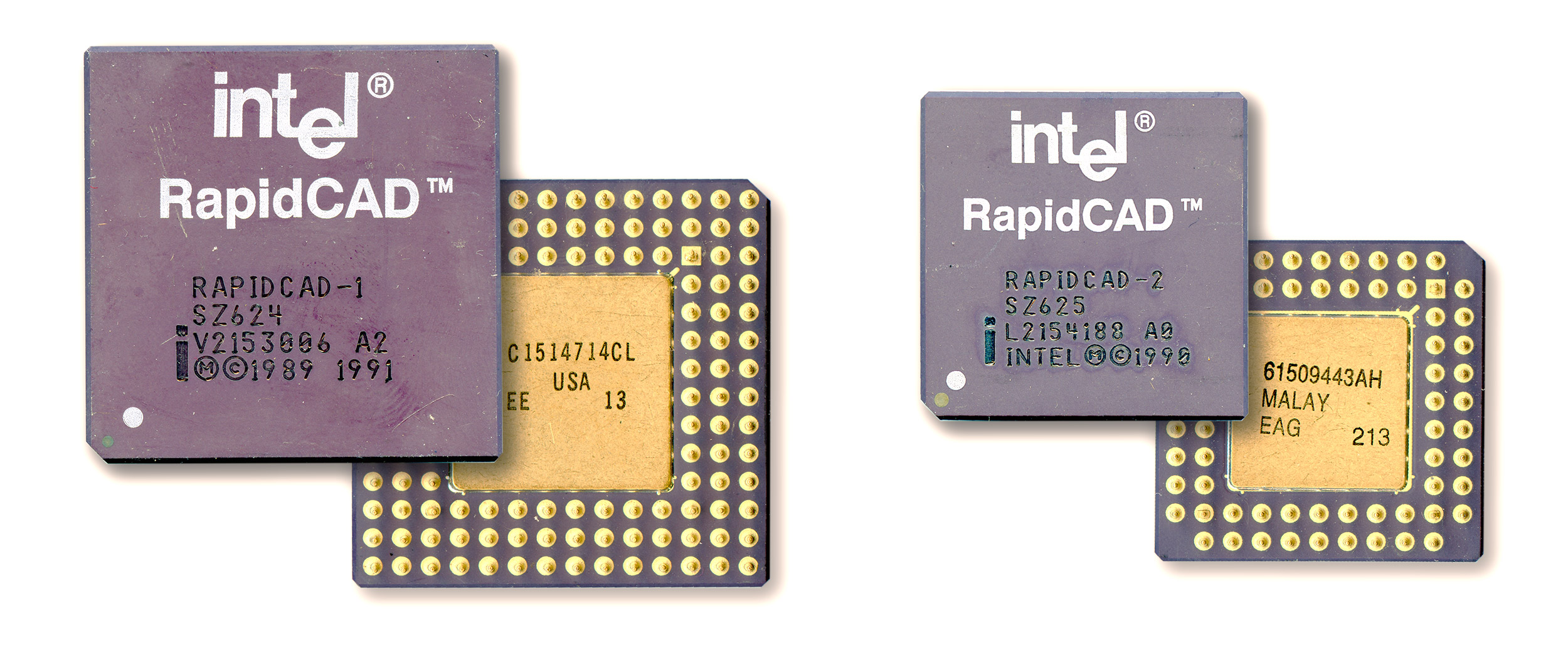
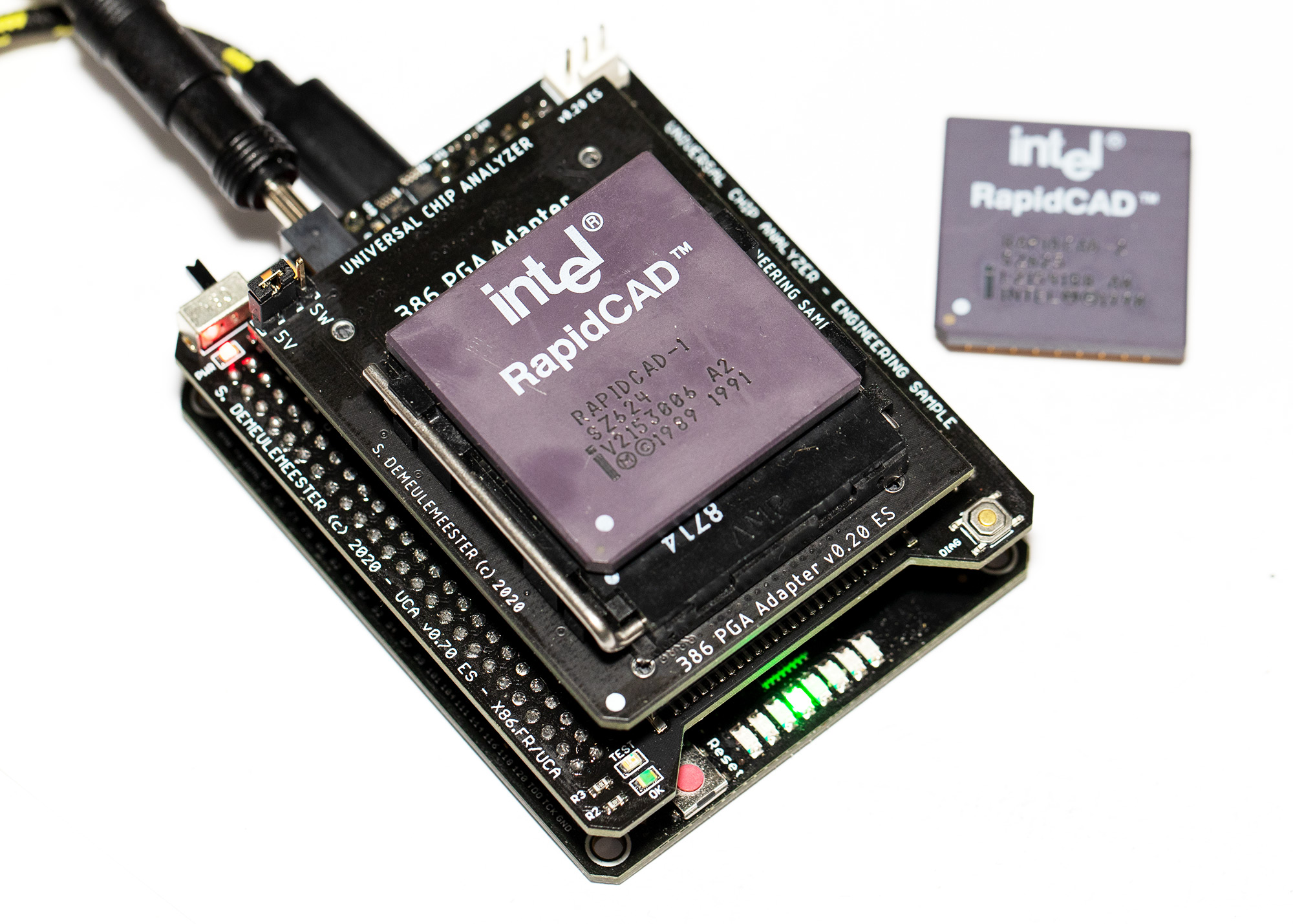
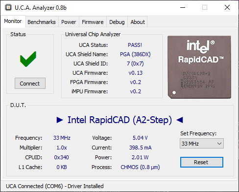
The elusive Intel RapidCAD Engineering CoProcessor is a weird and rare 2-chip set designed to upgrade 386 computers. It has been released in February 1992 for $499 and sold as a coprocessor. Technically, the RapidCAD is a 486DX assembled inside a 132-pin ceramic package that plugs into a standard 386 Socket. It features an integrated FPU but Intel removed the 8KB L1 cache and the 486-specific instructions. A second chip (RapidCAD-2) plugs into the 387 Socket, is only needed to provide the #FERR signal used to handle FPU exceptions.
This early sample has been assembled in April 1992 with dies from December 1991. The RapidCAD is able to work at any frequencies from 16 to 33 MHz. The lack of L1 cache and the slower 386 bus used does not provide a significant boost in Integer performances, but the FPU is the fastest available for 386s. The Universal Chip Analyzer is now able to fully test RapidCAD up to 33 MHz.
For some reasons, my sample was unable to run at 12.5 MHz, but works fine from 16 to 33 MHz. It’s probably due to the modification on the internal PLL needed to adapt a 486 CPU (1x clock signal expected) to a 386 Socket (2x clock required). PLLs often have limited top/bottom frequency lock range.
The reported CPUID is 0x340 and the power consumption is quite high (~2W typical in INT, ~2.5W in FPU) for a 386. I ran some INT benchmark only at 33 MHz and I got a score of 105.7 while a standard Intel 386DX-33 (or Am386DX-33) got 99.6. That’s only a 6% increase. The RapidCAD is much faster on FPU, being up to 70% faster than an Intel 387.
As like all previous microprocessors, Intel licensed the i386 design to third parties. AMD was the only one legally allowed to sell Intel-based 386s to customers (as bare CPUs), but IBM was granted the right to produce some Intel 386s for its own use. They don’t look like a standard ceramic CPUs : IBM used a plastic substrate and a metal cover to protect the die and help with thermal dissipation. Here is how they look like.
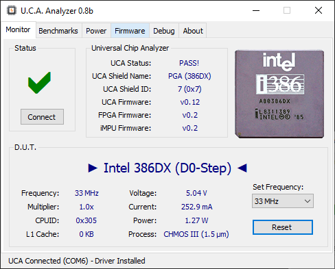
If the packaging is different, the internal die is the same as on Intel 386s. 7 different IBM part-numbers are actually known: 23F7189 (?? MHz), 32G6633 (25 MHz), 51F0352 (20 MHz), 51F1783 (20? MHz), 51F1784 (20 MHz), 51F1797 (25 MHz) and 63F7615 (25 MHz).I was able to put my hand on a 51F1784 and the later 63F7615. I tested both on the Universal Chip Analyzer. There is no “Pin 1” mark so I had to guess where is pin 1. Fortunately, the UCA has strong over-current and short-circuit protection. Let’s start with the 63F7615 :
This one is able to work fine up to 33 MHz, with a CPUID set at 0x305, similar to Intel 386 based on the D0-stepping. I don’t know for sure the real rated frequency, but it’s probably only 25 MHz. The other one (51F1784ESD) is not able to work at 33 MHz and not even at 25 MHz. The actual (early) UCA firmware only has 16/25/33/40 MHz, so I can only confirm that that my 51F1784ESD works at 16 MHz but not at 25 MHz. According to various sources, it’s probably rated at 20 MHz.
AMD Am386
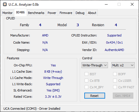
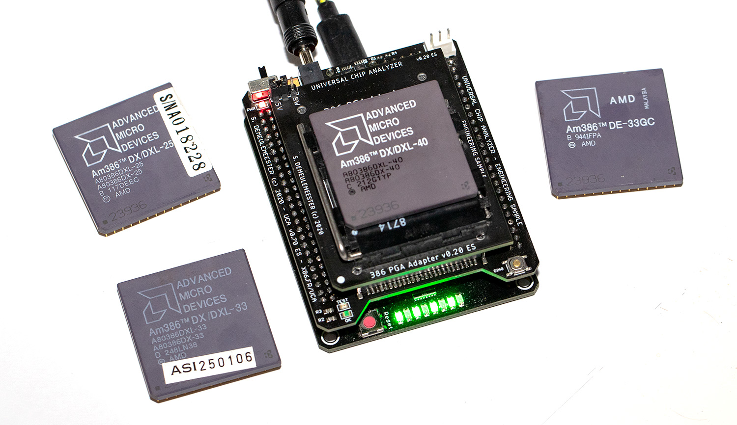
AMD also produced a lot of Am386DX at 20, 25, 33 and 40 MHz. While the microcode is 100% from Intel, the manufacturing process is different and they had lower power consumption (thanks to the 0.8µm process used by AMD instead of Intel’s 1µm CMOS-IV on the latest i386s).
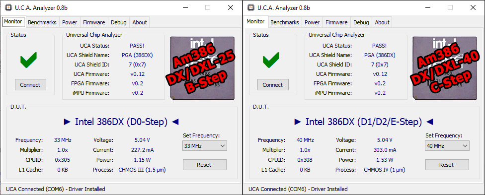
Let’s start with the standard Am386 DX/DXL. I tested one Am386 DX/DXL-25 “B-Step”, one Am386 DX/DXL-33 “D-Step” and another Am386 DX/DXL-40 “C-Step”. All came in the 23936 package from Kyocera.
The UCA tool is not yet able to detect them as AMD, but I’m working on a new algorithm based on power consumption to distinguish them from Intel 386s. The B-Step identifies itself as 0x305, the same CPUID used on Intel’s 386 D0-Step. The DXL-25 was able to work up to 33 MHz. Both C- and D-Step have a CPUID set at 0x308, like the later Intel 386s (D1 step and up).
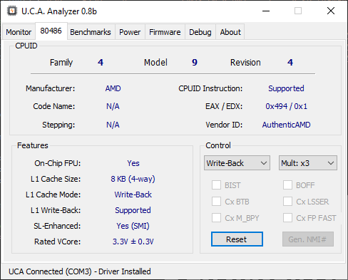
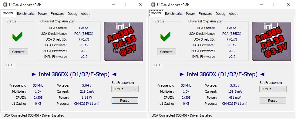
The last CPU to try was the Am386DE-33, an uncommon embedded model. Like the Am386DXL, it uses a fully-static design, meaning it can be clocked down to DC (0 Hz) while retaining all its internal registers content. The biggest difference between the usual Am386DX/DXL and the Am386DE is the disabled Paging Unit in protected mode on the latter. Bit 31 of CR0 (used to enable paging) is reserved on Am386DE. Another difference only available on the Am386DE is the ability to work at its rated frequency with a much lower voltage (down to 3.0V). And it works fine:
At 3.3V, the power needed drops by a huge margin, from 1.1 Watt to as low as 461 mW (0.46W). That’s a -60% power reduction!
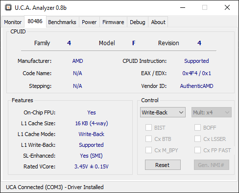
Another milestone has been reached. A new iconic CPU family is now supported by the UCA: the Intel 80386, the very first 32-bit x86 microprocessor! The i386 was originally released in 1985 at 12.5 MHz and 16 MHz. It added a 3-stage instruction pipeline and an on-chip MMU (Memory Management Unit) able to address up to 4 GB of RAM. A giant capacity for that time. The original Intel 386 – then renamed 386DX – comes in a PGA132 package and its frequency was later upgraded to 20 MHz, 25 MHz and finally 33 MHz. Later clones from AMD & Cyrix – not yet supported by the UCA – were also released at frequencies up to 40 MHz.
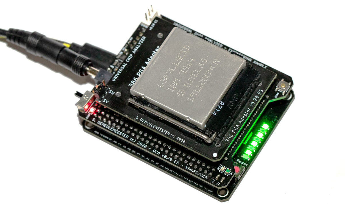
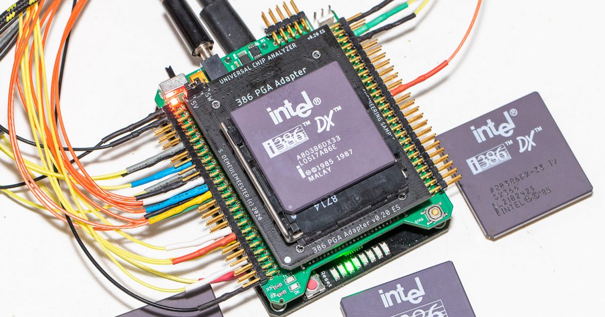
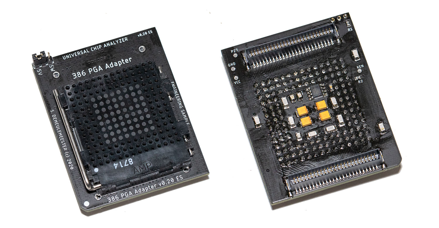
The design of the UCA 386 Adapter was challenging because of the high frequencies involved. While all 486s work with a standard clock input, 386s require a clock-doubled signal with a strong voltage swing (CMOS) between 0 and +5V. Generating frequencies up to 80 MHz (for a 386DX-40) with these requirement was not possible with the UCA architecture, so the UCA 386 Adapter includes an external clock-doubling PLL. For the first try, I used a NB3N511 clock multiplier from On Semiconductor but I was unable to reliably run 386s at more than 20 MHz. The UCA is based on a FPGA and timings are crucial. With the NB3N511, I was unable to successfully match timings because of the lack of phase synchronization between the input clock generated by the FPGA and the doubled frequency fed to the CPU. So I needed another PLL, with 0-delay between input and output.
After some research, I gave the ICS570A a try and it worked perfectly fine. I was able to sync the internal FPGA logic to the clock-doubled CPU signal up to 40/80 MHz, without having direct access to that signal. Some high-quality ceramic decoupling caps were also mandatory to achieve the highest frequencies. I had a bad surprise while looking at ZIF socket for the 386 Adapter: for some reasons, PGA132 ZIF Socket are extremely expensive and I was unable to source them at a decent price. I bought some at ~$25 each, but if you can help me find more at a lower price, please drop me an email!
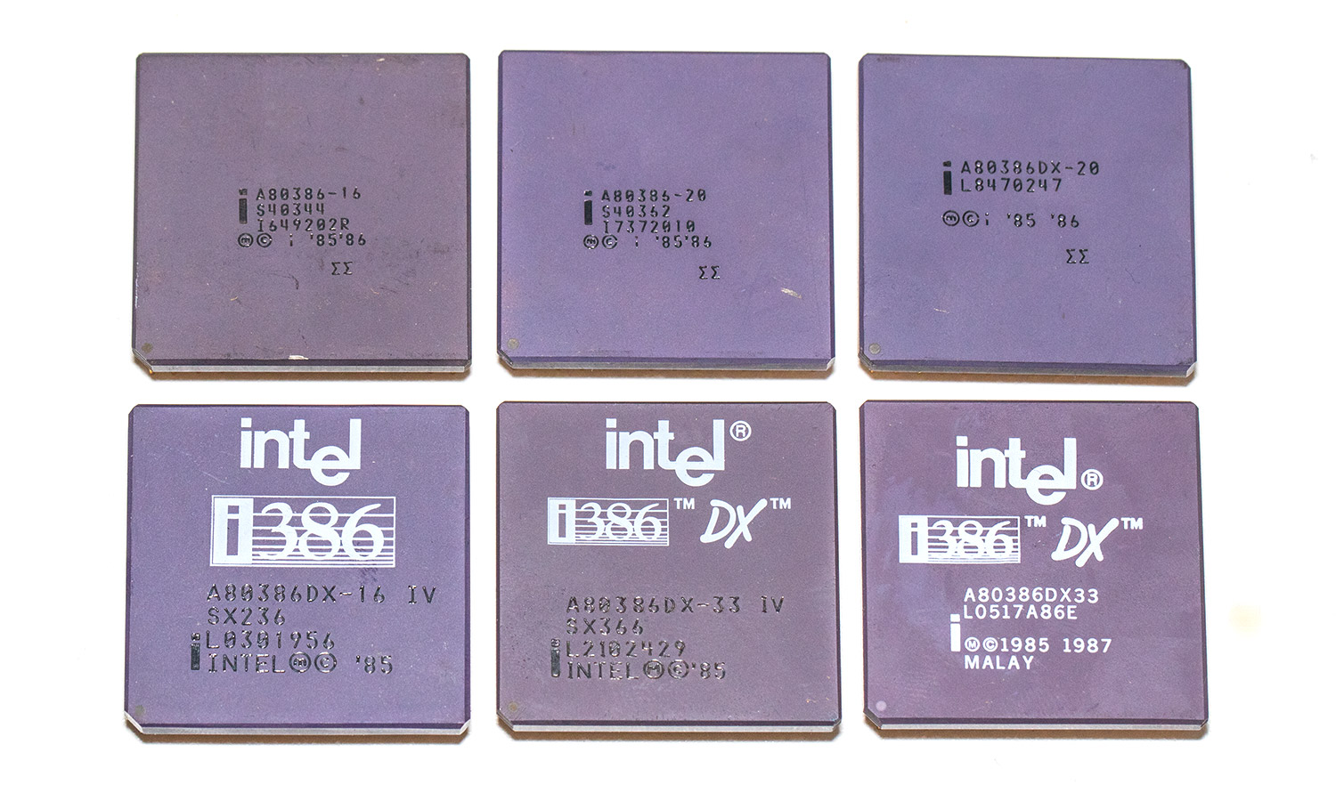
The 4 standard test frequencies for 386 are set to 12.5 MHz, 25 MHz, 33 MHz and 40 MHz. Right now, only Intel 386 are supported, but I’m working on AMD, Cyrix, etc. clones and I’m confident the UCA will support them all very soon. Here are the i386 I have for testing:
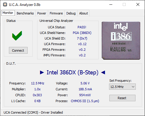
The first one is an early 386 clocked at 16 MHz and produced in 1986. The ΣΣ sign engraved shows that it has been tested free of the infamous 32-bit multiplier bug (more on this on a later post). According to this source, the S40344 S-Spec is a B1 stepping. This is confirmed by the CPUID displayed by the UCA Analyzer tool: 0x303. At 12.5 MHz, this CPU requires about 188 mA at 5V (a bit less than 1W).
The second one is very similar to the first one, except the rated speed at 20 MHz. Still the same B1-Stepping, same CPUID, same ΣΣ, same power consumption, same everything. It also can’t be overclocked at 25 MHz.
.
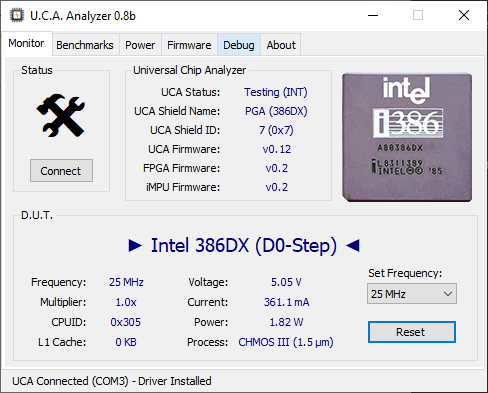
The third one is also rated at 20 MHz but don’t have any S-Spec. It has been assembled in November 1988, more than one year after the previous one. The CPUID is different at 0x305, which indicates a D0 stepping. Surprisingly, the power consumption is 10% higher, at ~212 mA for 5V at 12.5 MHz. Maybe Intel added some logic to solve the numerous erratas in previous stepping, maybe it’s just sample variation. Anyway, the D0 stepping still uses the CHMOS III (1.5 µm) process. This chip can be overclocked at 25 MHz
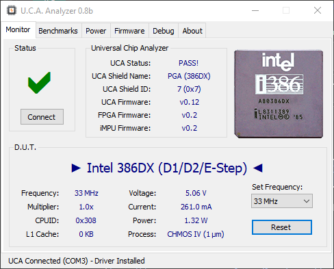
The fourth one is a 16 MHz marked SX236 and build with the more advanced CHMOS IV process. The CPUID is 0x308, which is used by Intel for D1, D2 and E Stepping. The last stepping is usually marked on the chip, so we can guess it’s a D1 or D2 stepping. Power consumption drops from 212 mA to 147 mA, thanks to the 1 µm process (instead of 1.5 µm). Unfortunately, it can’t work at 25 MHz.
.
The fifth one is a A80386DX-33 made in 1992 with s-spec SX366. It’s the faster clock speed Intel released for a 386DX. The CPUID is still set at 0x308 but the stepping is clearly more advanced: the power consumption drops to 126 mA while using the same CHMOS IV process than the previous one. This particular CPU requires 126 mA at 12.5 MHz, 206 mA at 25 MHz and up to 261 mA at 33 MHz. It can’t be overclocked to 40 MHz.
The last one is much newer than the others. It was manufactured in 2000 and uses the E-Stepping, as stated by the last letter of the lot code. Aside from this, all specs look identical to the SX366. Measures are also the same and it doesn’t work at 40 MHz.
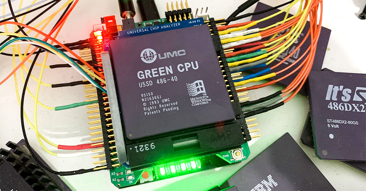
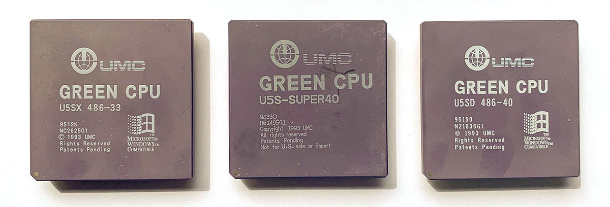
Last but not least, UMC’s 486s can now be tested on the Universal Chip Analyzer. All 486s ever manufactured are now supported! UMC is a Taiwanese semiconductor company still active today, albeit much smaller than its well-known competitors (TSMC, GlobalFoundries, …). In the mid-90s, UMC produced some rare 486s compatible CPU named “UMC Green CPU”. They were in-house design and not Intel-licensed like AMD 486s. Almost immediately after the initial announcement in 1993, Intel sued UMC and its distributors over patent infringements (including the infamous ‘338 patent, read more here). In response, UMC filled an anti-trust suit against Intel, but finally choose to give up and cease production of x86 compatible CPUs. Here are the retail UMC 486s I have:
The most common one was the U5SX (sometimes marked U5S) clocked at 25, 33 or 40 MHz and without FPU. Some UMC Green CPUs labeled “U5SD” were also released. Contrary to what you might think, they don’t include a FPU – verified with the UCA – but are just supposed to use the “DX pinout”. The meaning of this mention is unclear because both the i486SX and the i486DX shares the same layout for non-FPU related pins. Some guys have claimed that the difference is a relocation of the NMI pin, but I have not noticed that. UMC also released extremely rare U5D (with FPU) and U486DX2 (clock doubled with FPU), but only a couple samples are known today worldwide.
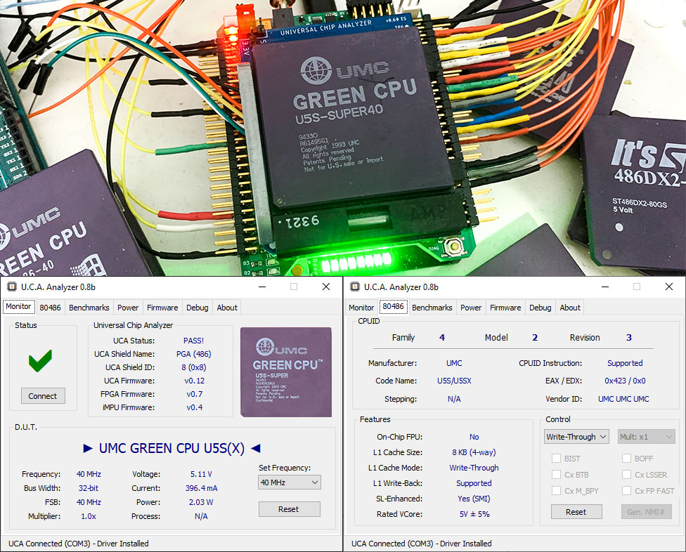
The Universal Chip Analyzer is able to test all UMC 486s, even if I still have an issue at 33 MHz and 40 MHz to grab every I/O. Code fetch works fine, but the output on I/O ports are sometimes dropped. It’s probably easy to solve, but I really need a copy of the UMC 486 manual / datasheet. Unfortunately, it seems nobody has one in the CPU collector’s community. If you can help, you’re more than welcome!
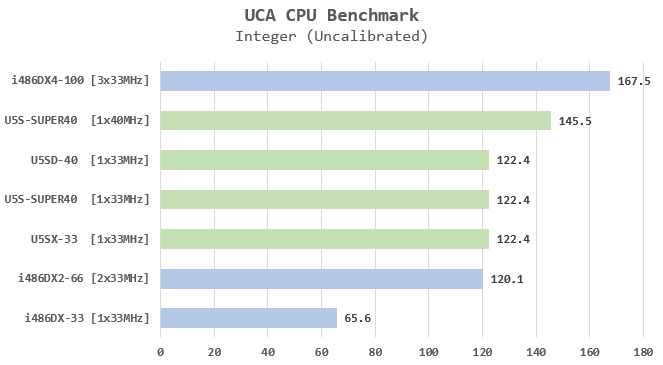
Looking at threads about the UMC 486 on cpu-world, vogons and vcfed, I saw that some people were wondering if the CPU marked “SUPER” were different from the “non-SUPER” ones. So, I ran some INT benchmark with the UCA.
As you can see, all UMC CPUs (U5S-SUPER, U5SX and U5SD) offer the exact same results when clocked at the same frequency. You also probably noticed the awesome relative performance of the UMC 486 versus the Intel 486s. Clocked at 33 MHz, the UMC 486 is as fast as an Intel 486DX2-66 and, when clocked at 40 MHz, it’s almost as fast as an Intel DX4-75. That’s not a bug. The UCA doesn’t have any wait-state on memory subsystem and actually uses a mix of heavy Integer divide and multiplication instructions for the benchmark. This result comes from the ultra-fast ALU designed by UMC, especially on divides. While Intel 486s requires 40 cycles to perform a INT divide, UMC 486s only need 7 cycles. That’s more than 5 times faster! However, in real-world applications, the UMC 486-SUPER at 40 MHz was on par with an Intel i486SX2-66. Still excellent!
In the 90s, Texas Instruments (TI) manufactured some 486-class CPUs under its own brand. TI was one of the third-parties who produced Cyrix processors (Cyrix was a fabless company). Consequently, the vast majority of TI-branded CPUs were just rebranded Cyrix 486s in PGA132 (386 pinout) or PGA168 (486 pinout). But Texas Instruments also designed its own 486 micro-architecture: the short-lived TI486SXL.
Good news: the Universal Chip Analyzer with the 486 adapter now supports all TI 486s!
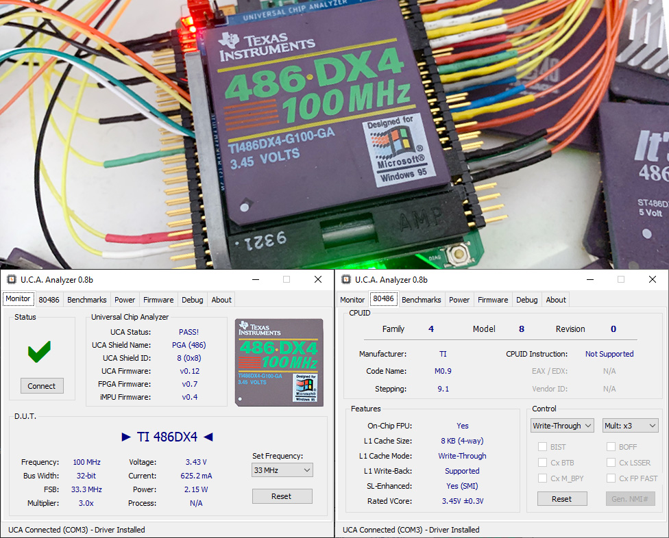
Let’s start with the fastest one, the TI486DX4-G100-GA.
The “Colorful” Ti486DX4 is a rebranded Cyrix 486DX4-100: clock-tripled with 8KB L1 WB cache. Compared to IBM 486DX4 or ST 486DX4, both also rebranded Cyrix, the Ti486DX4 includes a tiny difference. IBM and ST CPUs are indistinguishable from a Cyrix CPU. Texas Instrument insisted to add a way to distinguish their CPU. This was implemented by setting a bit (DIR1[7]) in one of the Cyrix-specific registers. If the bit is “1”, the CPU is Ti-branded. If the bit is clear, it’s a Cyrix, IBM or ST 486. Other than that, nothing changed.
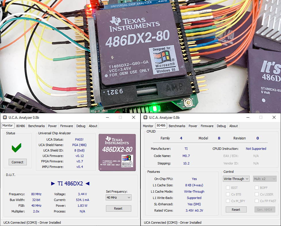
TI also released some 486 DX2, like this TI486DX2-G80-GA.
Again, it’s just a rebranded clock-doubled Cyrix 486DX2 with a specific identification bit set. The DX2-80 seems more common than the DX2-66. The Universal Chip Analyzer is perfectly able to test it at 2×40 MHz.
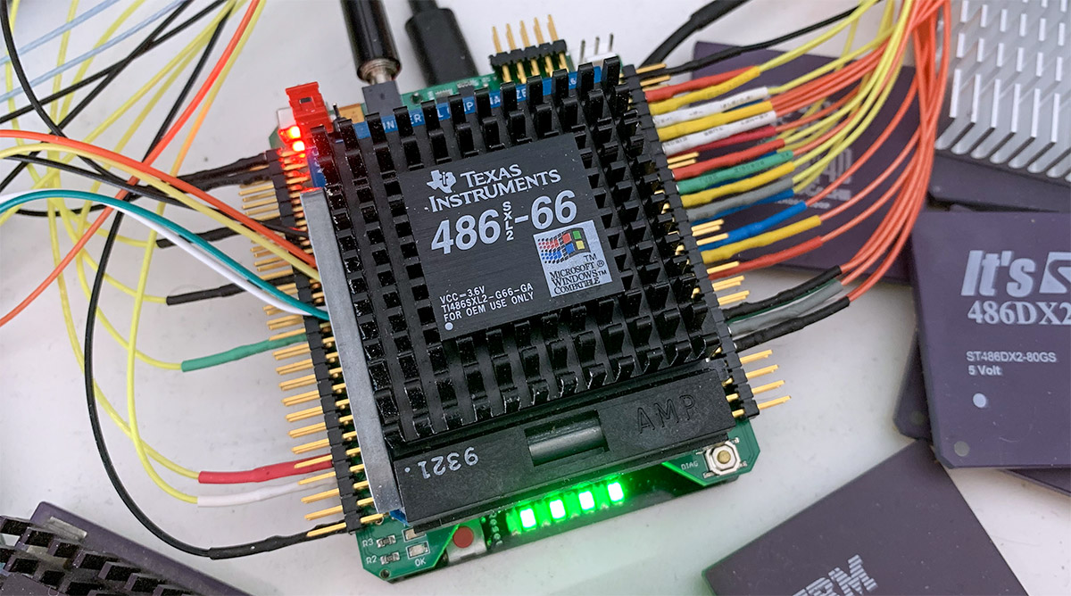
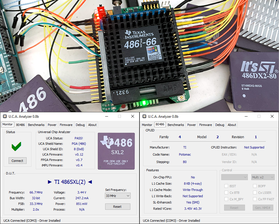
But the most interesting Texas Instruments 486s are the ones based on their own micro-architecture like this TI486SXL2-G66-GA.
Codenamed “Potomac”, this clock-doubled CPU with 8KB of L1 cache doesn’t integrate a FPU. Ti was probably thinking of developing a FPU later. The mechanism to enable the clock-doubled PLL is different than all other CPU, who uses a specific pin to toggle between 3x and 2x (DX4s) or just boot at 2x by default (DX2s). The Ti 486SXL2 powers up in the non clock-doubled mode. To enable the 2x PLL, you have to write a specific bit in a proprietary register called CCR0 (with the same mechanism involving reading/writing to port 0x22h/0x23h as on Cyrix 486s). Setting bit 6 on CCR0 switchs on the clock-doubling PLL instantly (within 20 µs). I was able to overclock this CPU to 80 MHz at 2×40 MHz (still at 3.45V).
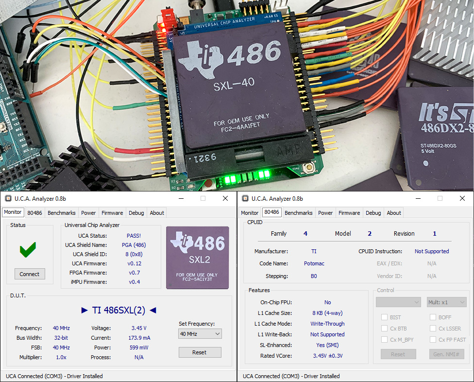
Texas Instruments also released non-clockdoubled “Potomac” CPUs like this Ti486SXL-40.
As you can see on the UCA Analyzer screenshot, it seems there is no way to distinguish them from SXL2 from a hardware point of view. Of course, it’s possible to check if the CCR0 bit 6 is set to 1 to know if clock-doubled mode is enabled, but the SXL2 can also work as a SXL in 1x mode.
While messing with CCR0 and the x86 code that run on the CPU, I found something very interesting: my SXL-40 also supports the clock-doubling mode! I had to run several benchmarks to be sure, but yes: that Ti486 SXL-40 can work as a SXL2 with the exact same power consumption and the same performances.
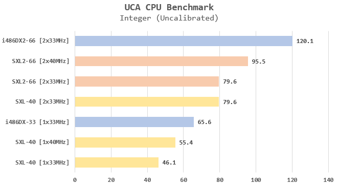
I used the preliminary Benchmark Mode on the UCA. These Integer scores are not calibrated so they’re only valid to compare these CPUs on a relative scale. We can see that the Ti SXL microarchitecture is ~30% slower than the Intel 486 one at equal clock frequency, but the SXL-40 is just 18% slower than a Intel 486DX-33. The Ti SXL2-66 is much faster then the DX-33, but the i486DX2-66 is far beyond.
Finally, it seems the SXL and SXL2 – at least on B0 stepping – are the exact same CPU. The B0 stepping is probably the only one that can work in 2x mode. “Potomac” A0 doesn’t support SMI and probably doesn’t have the integrated PLL. I also tried to activate the 2x mode and keep the 40 MHz FSB on the Ti486SXL-40 and … it works, actually doubling the performance (similar to a hypothetical “486SXL2-80”).
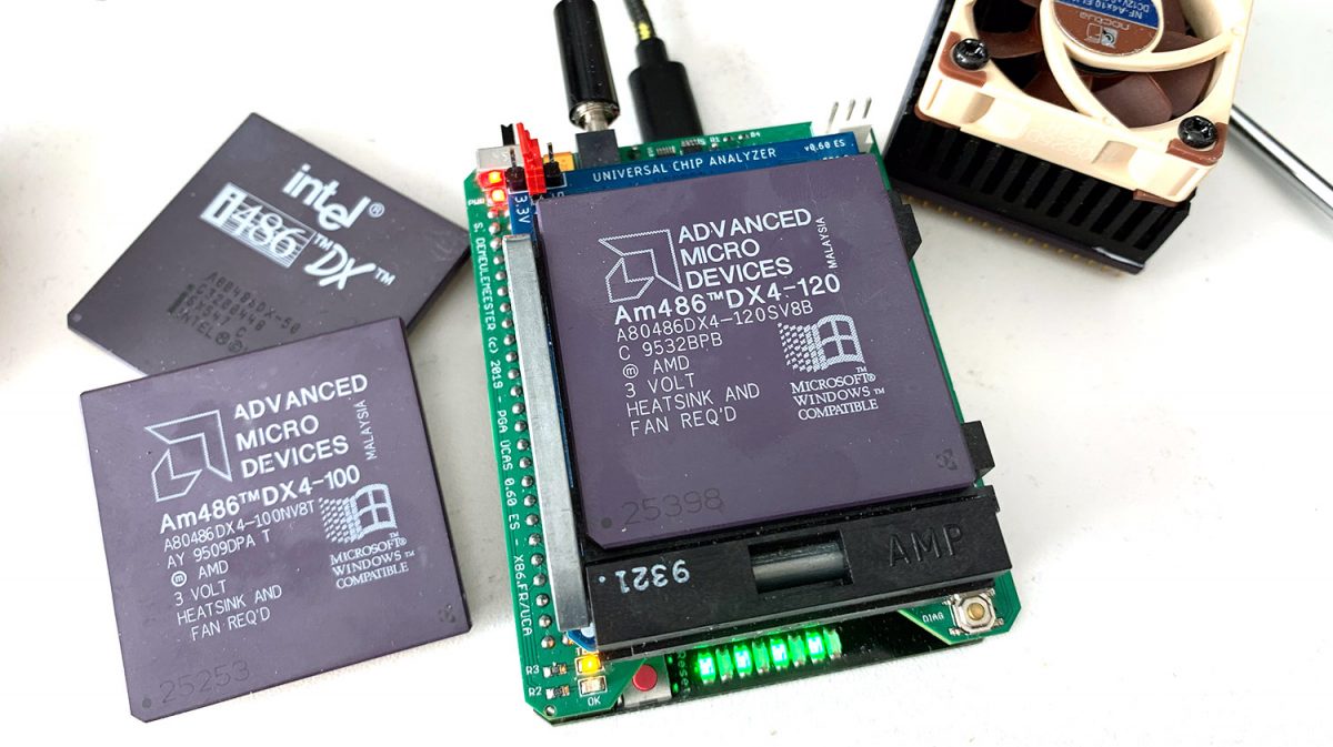
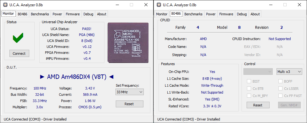
While I was adding support for AMD CPU on the Universal Chip Analyzer, I spotted what looked-like a strange chip at first sight. I was then working on the L1 cache size detection, to distinguish between CPUs with 8 KB and others with 16 KB. In their BIOS Development Guide, AMD wrote a specific code that checks the status of a tag bit in a test register (TR4). After implementing this test path in the x86 code run by the CPU on the UCA, I needed a CPU with 16 KB L1 cache to try on 486 (5x86s were OK). I found this uncommon Am486 :
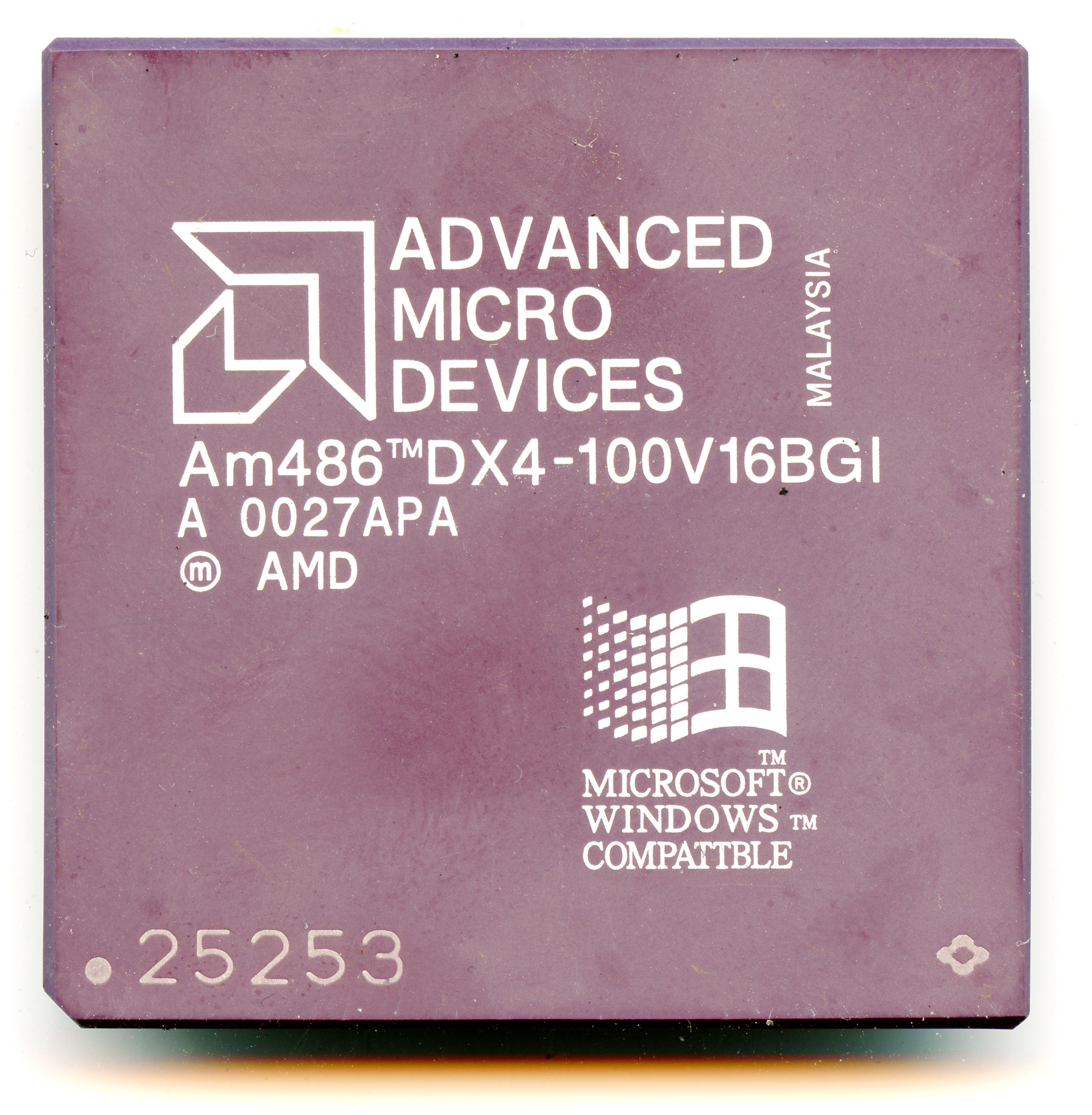
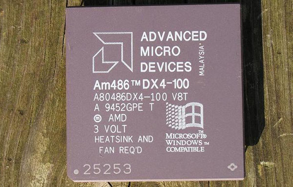
This is a nice Am486 DX4-100V16BGI. This part number decodes as follows: A clock tripled (“DX4”) CPU rated at 100 MHz (“100”) and 3.3V (“V”), with a 16 KB (“16”) Write-Back (“B”) L1 cache in a 168-pin PGA package (“G”) and qualified at Industrial temperature range (“I”). This last point is uncommon because the vast majority of Am486 are “Commercial” grade (0°C to 85°C) and not “Industrial” (-40°C to +100°C). That’s probably why I bought this CPU years ago.
But the AMD code was not working: the size of the cache detected was 8 KB instead of 16 KB. I began to have doubts about the genuineness of this CPU. I started to play with the UCA. No way to enable Write-Back: the CPU stays in Write-Through Mode and the CPUID does not change accordingly as on “SV8B” AMD 486s. This CPU does not support Write-Back. I suspected a remarked early “NV8T” DX4-100, but that was not the case: they come with a CPUID 0x484 and this CPU was 0x482 in 3x Mode and 0x432 in 2x Mode.
I was able to find a very early Am486DX2-80 V8T (notice the lack of “N”) manufactured in 1994 with the first A-Stepping. The UCA detects a CPUID set at 0x432, which match with my fake DX4 (in 2x Mode). Early Am486DX4-100 V8T also exists with a CPUID 0x482 in 3x Mode. Some of them seem to have been later remarked to Am486 DX4-100V16BGI.
On closer inspection, several points should have caught my attention about this CPU. No way to be certain of what it really was without the UCA, but the fact that it was a fake could have been known sooner.
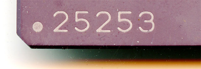
Package code is wrong
The AMD package code is written in bottom left of all AMD CPUs from this era. The first AMD Am486s like the Am486DX-33/40 or very early Am486SX2/DX2s use the “24361” package. Later 486DX2 “V8T” and “NV8T” CPUS come in the “25220” or “25253” package. Enhanced “SV8B” DX4s (with SMI and Write-Back) are assembled with the “25398” package. Then we have package “25498” for newer CPUs like the Am486DE2. Later models (SV16B and 5×86) use the “25544” package”. This later one was expected for a genuine Am486DX4-100V16BGI, but the fake CPU comes with an old “25253” (N)V8T package.
Package code is “25253”, similar than old (N)V8T Am486
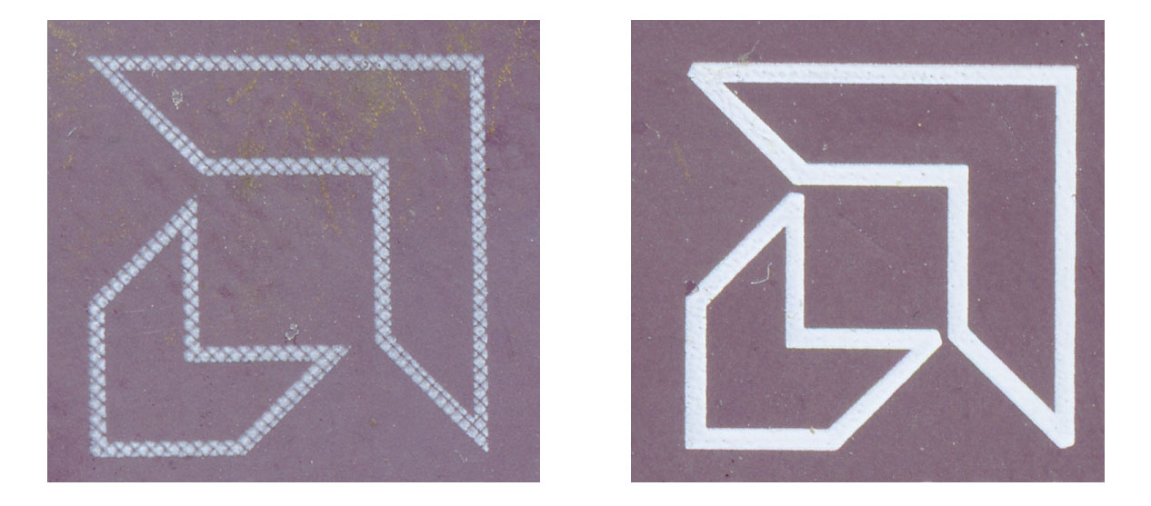
Markings without hatching
As you can see in the picture below, AMD markings on CPUs from this era use a typical hatching pattern. This pattern is not present at all on the fake CPU.
Marking error
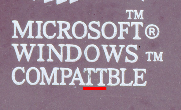
But the most obvious error is a big mistake on printing. Here you can see the word “COMPATIBLE” is actually spelled “COMPATTBLE”, with a double “T”.
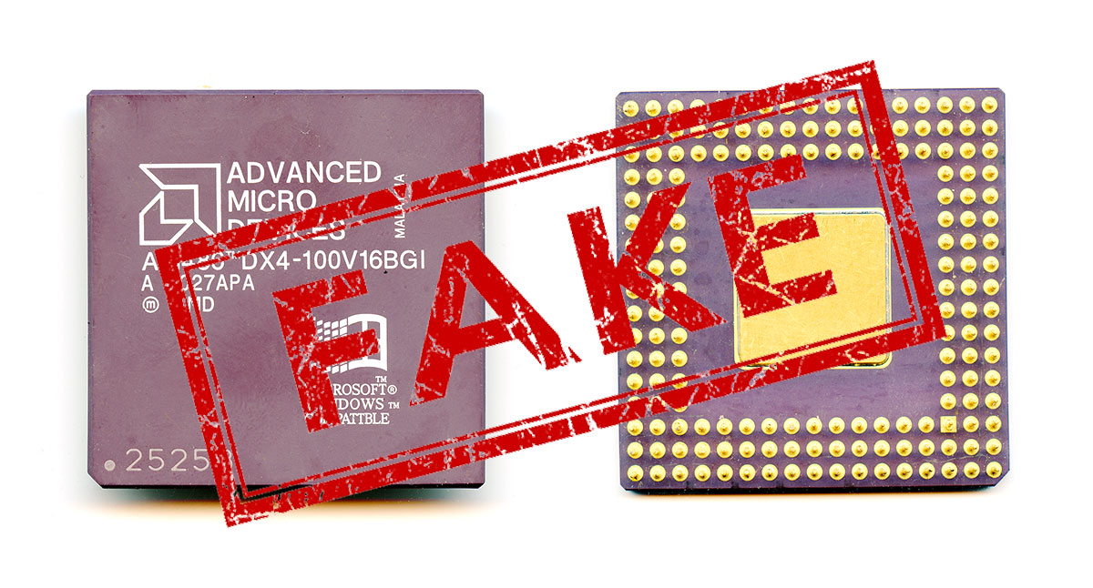
There is no doubt at this point that this CPU is a counterfeit Am486DX4. The only question remaining is when was it remarked by fakers? Counterfeits CPUs – especially 486s – were common in the 90s to boost frequency, but here, the original CPU was already an Am486DX4-100 (albeit a very early one with 8 KB L1 Write-Though Cache, instead of the expected 16 KB L1 Write-Back Cache). More recently, in the mid-2010s, old CPUs from the 90s were also faked to target CPU collectors all over the world.
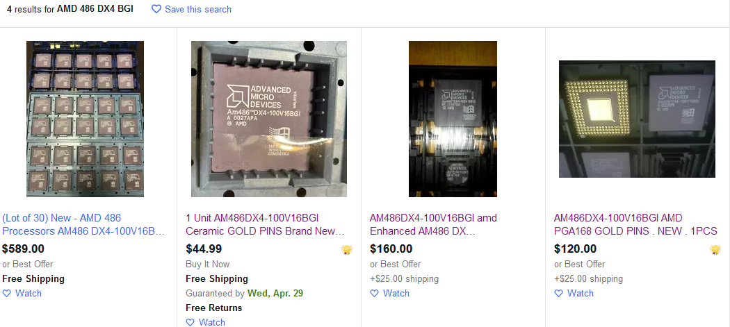
Looking at eBay listings right now (2020-04-23), I found 4 vendors selling Am486 DX4-100V16BGI for a (very) high price. Two of them – including one who only sells multiple 30 pcs lots – are obviously the same fake as the sample analyzed here. The other two look different but still highly suspicious, with a Windows Logo not on par with the unusual Windows printing from AMD for the first one, and a very odd font for the second one (seems also marked “COMPATIBLF”)
Along with AMD, Cyrix was one of the biggest Intel challengers in the 486 era. While most of the AMD Am486s used the exact same microcode as Intel 486s, Cyrix was the first to release a 100% compatible processor based on a custom design. Being a fabless company, Cx486s were manufactured by IBM, ST Microelectronics and Texas Instruments. All of them sold Cyrix 486s under their own brand.
Adding support for Cyrix-based 486 and 586 was more challenging than expected. As many of you probably remember, 486 motherboards were full of jumpers because of the many different pinouts. I want the UCA to be able to test every CPU out of the box without messing with jumpers, so I had to use many tricks to accommodate the different pinouts. I also wasted a lot of time trying to understand the erratic bugs I had when adding more x86 code to detect Cyrix CPU. The cause was finally obvious, but I had a hard time spotting it: two address lines (A11 & A9) had been inverted in the FPGA code for more than one year!
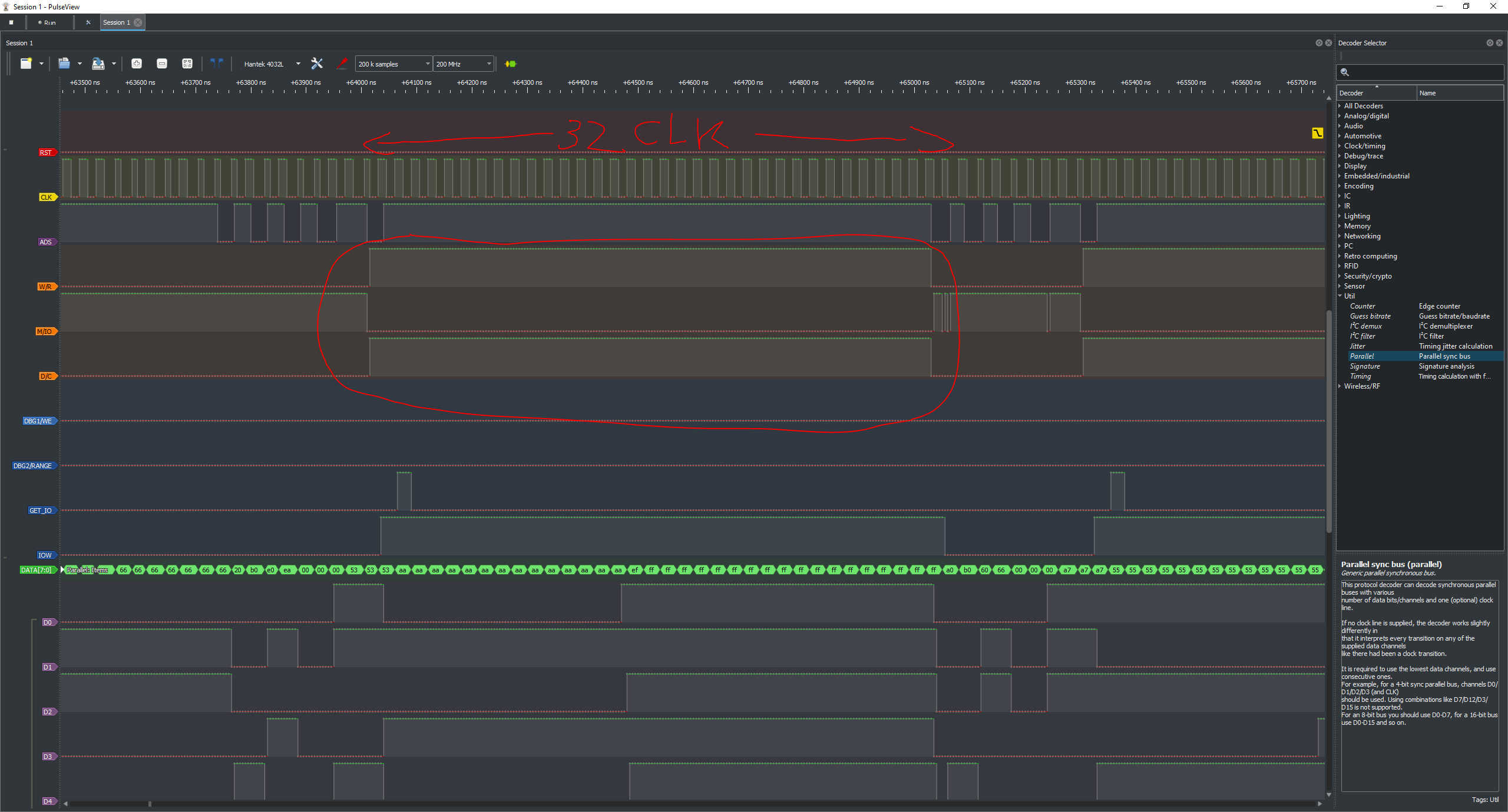
This stupid typo came on top of another Cyrix-only specification I had to deal with. All the HDL code I wrote for the UCA is focused on achieving 0 wait-states. Unfortunately, when I started to work on support for the Cx486, it crashed almost instantly, even at low frequencies. I rewrote a lot of Verilog to achieve near-perfect timing, matching the original Intel datasheet almost perfectly. But the Cx486 kept crashing. I had to wire everything to my 32-channel logic analyzer to understand why all Cyrix 486s failed to work on the UCA. The answer is shown on this screenshot:
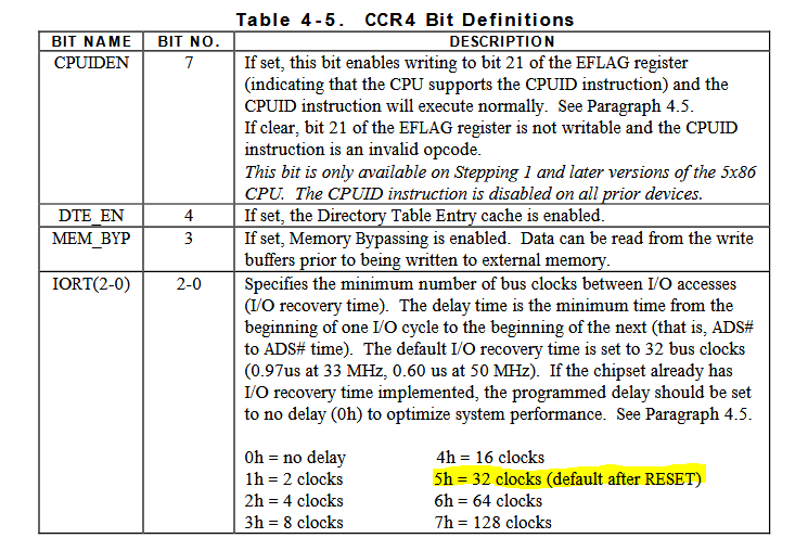
Cyrix added an unexpected (normally chipset-related) mechanism that adds hardware wait-states to every I/O. And not just a couple of them: 32 clock cycles for every I/O by default! The state machine that handles the decoding of CPU cycles inside the FPGA wasn’t able to understand why the CPU doesn’t resume operation after an I/O and assumes a timeout has happened. As soon as I changed the HDL code to handle this case, Cyrix CPUs started to work properly on the UCA. I could have saved myself a lot of effort if I had RTFM more carefully: this behavior is indeed described on the 5×86 CPU BIOS Writer’s Guide, page 12:
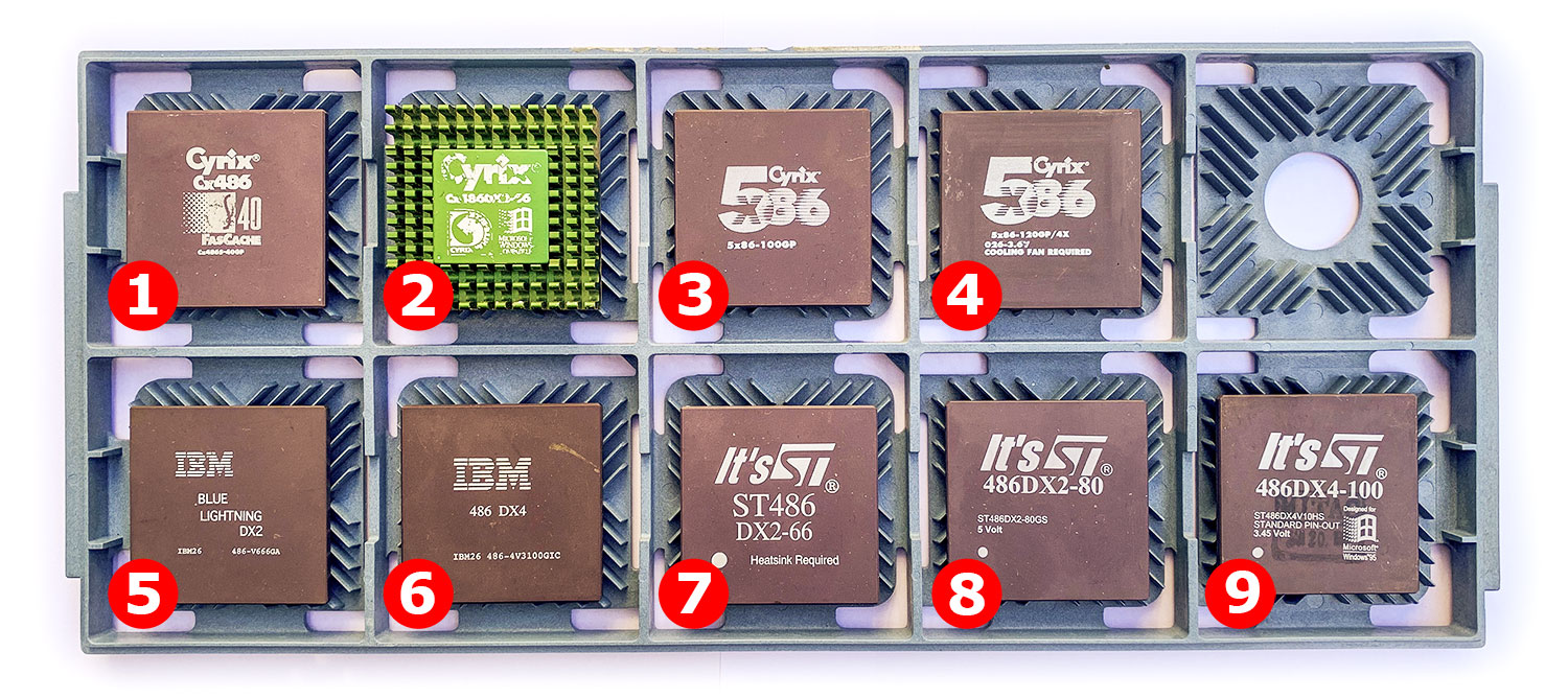
Maybe I’ll add a software path later to change this setting with the UCA Analyzer tool. Messing with Cyrix-specific internal registers on the fly is an upcoming feature already planned! As with AMD, I grouped all the non-ES Cyrix CPUs I had in a tray and starts testing.
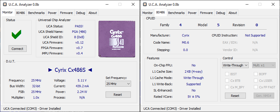
(1) Let’s start with the Cyrix Cx486S-40, one of the first 486-class CPU released by Cyrix in March 1993. It features 2 KB of write-back L1 cache, quite unusual for the time. The CPUID at reset is 0x450, which does not correspond to any Intel 486 (i486SX are 42x). Power consumption is quite high. Also note that the screenshot is done at 25 MHz for a rated maximum clock of 40 MHz. For an unknown reason that deserves a longer investigation, very early Cyrix 486 like this one cannot run at 33 MHz or more on the UCA with the actual HDL code. Maybe it’s due to the added electrical interference from the Logic Analyzer, or maybe It comes from a regression in the code after I messed with timings, but that Cx486S-40 was able to run at 40 MHz some days ago, so I’m quite confident It will be fixed soon. I was just too lazy to unwire everything to take the screenshot.
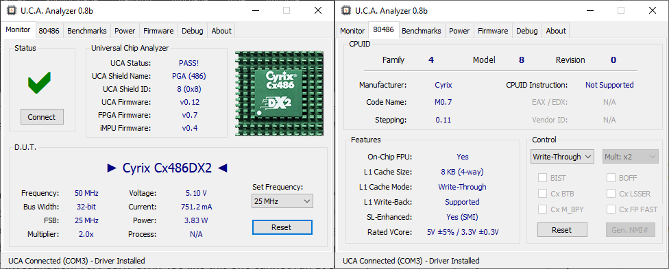
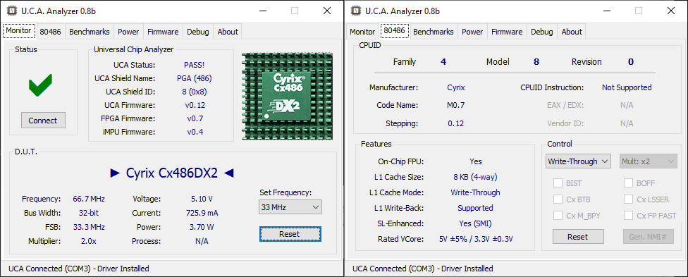
(2)Cyrix Cx486DX2-66. A clock doubled 486 with FPU. CPUID after reboot is 0x480 (similar to Intel DX4s) but the CPU does not support the cpuid instruction. Cyrix CPU has two registers named DIR0 and DIR1 for identification. This one contains 0x1B in DIR0, the hex value for a Cx486DX2. DIR1 contains 0x0B. DIR1[7:4] is “CPU Step Identification Number” (here 0x00) and DIR1[3:0] is “CPU Revision Identification” (here 0x0B or 11 in decimal). The actual “Cyrix stepping” is 0.11. This CPU is marked A3CM434M and has been manufactured week 34’1994. It’s an early example. Like the Cx486S, it does not work at more than 25 MHz on the UCA yet (but it will soon).
(5)IBM “Blue Lightning DX2” 486-V666GA. An IBM-branded Cyrix 486DX2-66. They are strictly identical from a microarchitectural point of view but are supposed to come with a stricter QC (Quality Control). This one is a 3.45-3.6V part, and not a 5V CPU like the previous one. It is also much newer (manufactured in March/April 1995). Stepping/Revision is 3.2. No problem running it on the Universal Chip Analyzer at 66 MHz (2 x 33.3 MHz).
(6)IBM 486 DX4 / 486-4V3100GIC. Well, I can’t remember where this CPU come from, but it doesn’t work. Not a single sign of life on the UCA not on a standard 486 motherboard. The power drawn seems linked to the clock signal applied (so the internal die is not shorted), but when wired to the logic analyzer, not a single pin toggles after reset. Unfortunately, it looks dead. 🙁
(7)It’s ST ST486 DX2-66. While IBM-branded Cx486s are often known for their higher QC (and higher overclocking), ST’s 486 are usually less overclockable. This CPU was manufactured in February 1995 but still uses the Stepping 0.12. A single step newer than the very old Cyrix Cx486DX2-66 but much older than the IBM Blue Lightning DX2. It works as expected at 66 MHz
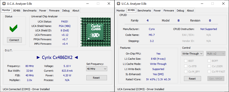
(8)It’s ST ST486 DX2-80. This part is very close to the IBM Blue Lightning DX2. It uses the same 3.2 Stepping but works at 5V instead of 3.45V. Power consumption is quite high (~4.5W) and it runs hot. CPUID is 0x480. No problem to have it running on the UCA at 80 MHz (2 x 40 MHz).
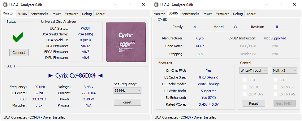
(9)It’s ST ST486 DX4-100. Very late 3.45V clock-tripled CPU manufactured in 1997. The stepping is 3.6, which corresponds to the latest Cyrix 486 revision ever produced. CPUID is still 0x480 and L2 cache is limited to 8 KB Write-back (instead of 16KB for latest Intel 486 DX4s). It runs fine at 66 MHz (2×33.3 MHz) and 100 MHz (3×33.3 MHz).
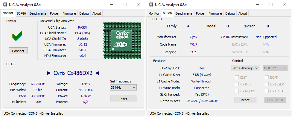
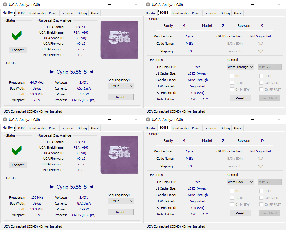
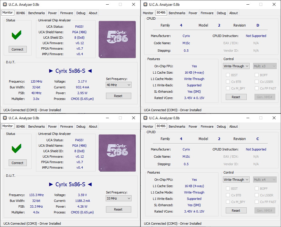
(3) Cyrix 5×86-100GP. The 5×86 is a short-lived, stripped-down version of the Cyrix 6×86. It features 16 KB of L1 Write-Back cache and a 5th generation (Pentium class) microarchitecture. The vast majority of 5×86 processors run at 2x or 3x multipliers. This example is a quite early “1.3” revision. CPUID changes from 0x429 at 2x to 0x42D at 3x. It can work on the UCA at 120 MHz (3×40 MHz) with 3.6V.
(4) Cyrix 5×86-120GP. Some late (and rare) 5x86s are able to work with a 4x multiplier (in addition to the default 3x multiplier). For some unknown reason, the revision/stepping drops to 0.5 even if the CPU was manufactured way after the previous one (in 1996). CPUID at 4x is 0x42C (and stay at 0x42D at 3x). Here is that nice 5×86-120 running at its rated 120 MHz (3×40 MHz) and then overclocked at 133 MHz (4×33.3 MHz) @ 3.6 volts
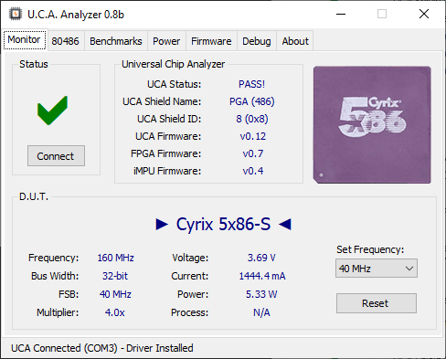
For fun, I also tried to increase the voltage to 3.7V before restarting the UCA at … 160 MHz (4x 40 Mhz) ! To my surprise, it successfully completed a test pass. I stopped to avoid any damage to the CPU, but that was probably the fastest pass ever run on the UCA.
Awesome!
Next step is to add support for the remaining 486 brands (and solve the frequency regression on early Cx486s). I also have a nice feature upgrade for the 486 adapter planned soon. Stay tuned!
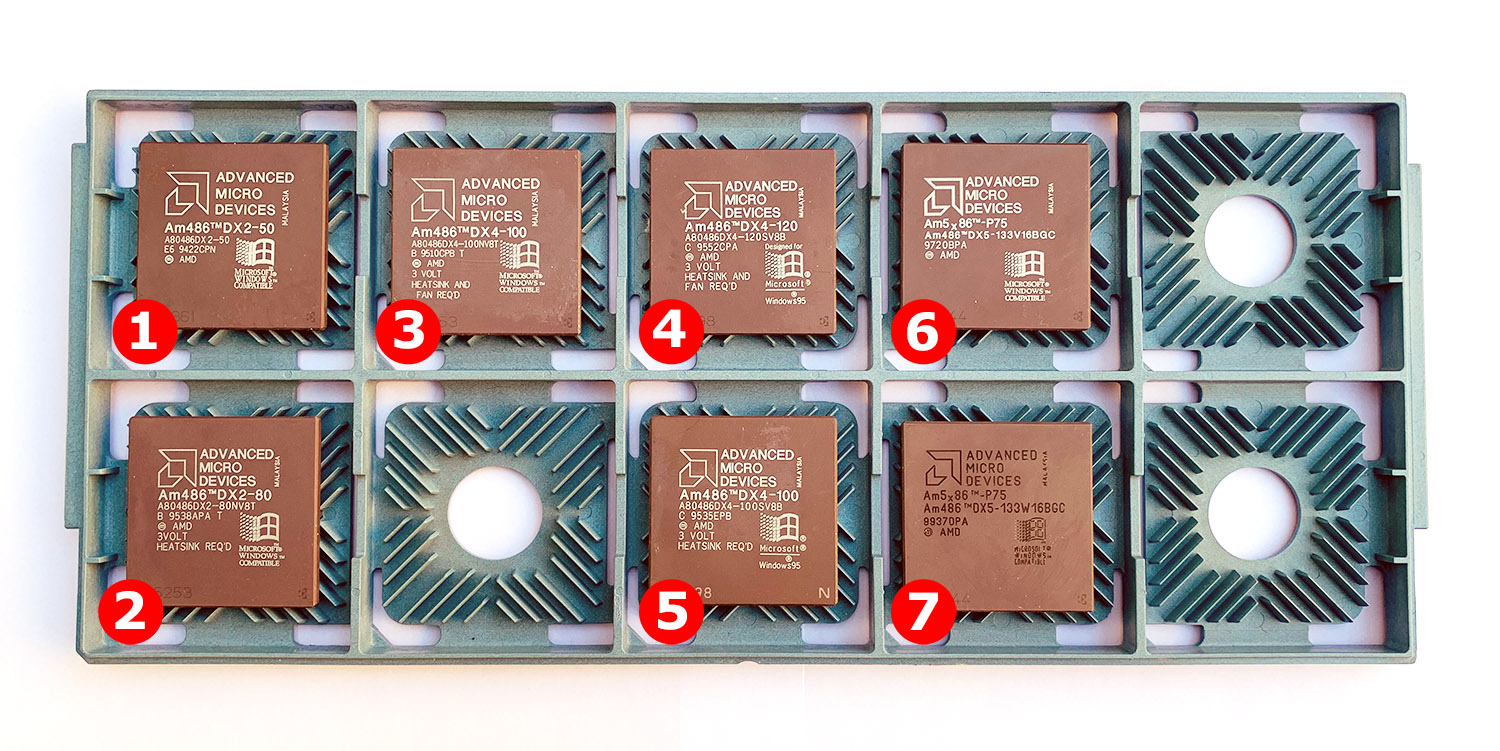
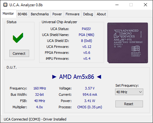
After the initial support for Intel 486s, the Universal Chip Analyzer with the new 486 adapter now supports all 486s from AMD. I’m an avid CPU collector but I only collect Engineering sample (check my collection here!). Of course, some analysis on these ES will be published here soon, but to add support for AMD 486s, I bought some “retail” Am486 and Am5x86. Here they are:Good news : they all work well on the UCA! Here are some notes I took while testing.
Am486DX2-50(1) – Am486DX2-80NV8T(2) : 8 KB L1 Write-Through Cache. Both CPUID 0x432 with cpuid instruction not supported. Virtually undetectable from Intel DX2 : Same microcode. Same power consumption. Exact same performances. Maybe distinguishable from Intel DX2 with JTAG. Work in progress on this point.
Am486DX2-80NV8T
Am486DX4-100NV8T (3) : 8 KB L1 Write-Through Cache. CPUID also 0x432 without cpuid instruction. Real nightmare to distinguish from Intel. B-Step a bit lower power (-5%) Vs AY-Step. INT Perfomance is lower than Intel DX4 (-20%). FP Performance almost identical. Power consumption is also lower (-25%). One interesting thing : In 2x mode, the CPU is exactly as fast as an Intel DX2. However, in 3x mode, it seems significantly slower than a DX4, but only in INT. Performances looks like 2.5x in INT (according to cycle count) and “real” 3x in FP. Strange. That deserves some additional investigation.
Am486DX4-120SV8B (4) – Am486DX4-100SV8B (5) : Newer core with SMI and Write-Back L1 Cache (still 8KB). CPUID instruction supported. 2x/3x Mode and WT/WB change CPUID (0x434/0x474 in 2x mode, 0x484/0x494 in 3x mode). Exact same performance than NV8T. Bit higher power consumption (+10%).
Am486DX4SV8B in 2x Write-Throught ModeSame Am486DX4SV8B, in 3x Write-Back Mode
Am5x86-P75 (Am486DX5-133V16BGC) (6). 16KB Write-Back L1 Cache ! CPUID instruction supported. 3x/4x Mode and WT/WB change CPUID (0x484/0x494 in 3x mode mode, 0x4E4/0x4F4 in 4x mode). INT Performance identical to 486DX4-100 (looks like INT units are locked in 3x mode). FPU performance are far better (real 4x). Doesn’t support overclocking to 160 MHz.
Am5x86-P75 In 4x Write-Back Mode
Am5x86-P75 (Am486DX5-133W16BGC) (7). Same than previous one, but supports overclocking to 160 MHz with 3.6V !
 Why not 25 MHz? Because the 80286 requires a clock-doubled input and feeding a 50 MHz clock to get the 25 MHz core frequency would have required an external PLL. Not a big deal, but there is only one rare 286-class CPU that supports this frequency (the Harris/Intersil CS80C286-25 pictured above) and its timings is not fully compliant with the 286 specifications. Designing a special UCA adapter just for this chip is trivial, but quite useless because the 286 Adapter is already able to test it at 20 MHz. Speaking about “high” frequencies, using the right socket is crucial
 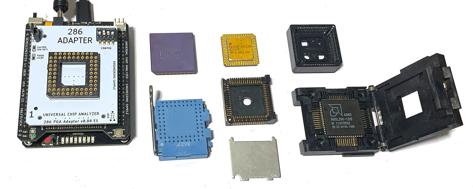 The UCA 286 Adapter is fitted with a high-quality DIP Socket. Directly plugging a PGA 286 CPU is possible but not convenient for testing multiple CPUs in a row. I was able to secure some ZIF Sockets for 68-pin PGA like the blue one pictured here (from AMP) and also some 3M LCC sockets complete with top cap. About PLCCs, I first tried some cheap socket from eBay. That was a disaster: contact pins were too weak and bent after 2-3 insertions. Worst, the maximum frequency allowed was 8-10 MHz. Replacing these crappy sockets with other ones from Foxconn or 3M solved all the issues. I also bought some awesome Yamaichi test Socket for PLCC (on the right), but unfortunately, they use a specific pinout. As the 286 Adapter uses a simple 2-layer PCB, I will consider designing a specific PCB just for them.
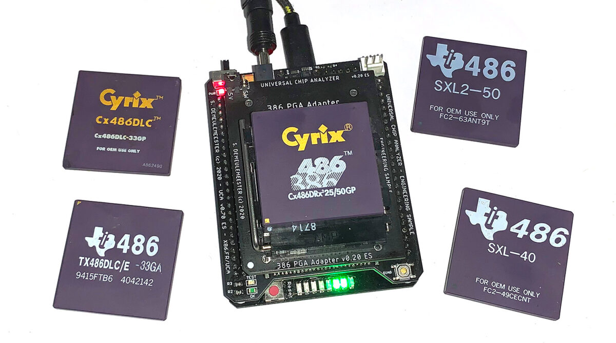


 There is no doubt at this point that this CPU is a counterfeit Am486DX4. The only question remaining is when was it remarked by fakers? Counterfeits CPUs – especially 486s – were common in the 90s to boost frequency, but here, the original CPU was already an Am486DX4-100 (albeit a very early one with 8 KB L1 Write-Though Cache, instead of the expected 16 KB L1 Write-Back Cache). More recently, in the mid-2010s, old CPUs from the 90s were also faked to target CPU collectors all over the world.